E3165_Sistem Elektronik Berdigit
279
E3165 / UNIT 1 / 1 PEMBINAAN GET LOGIK ASAS Objektif Am: Mengetahui dan memahami pembinaan get-get logik. Objektif Khusus: Pada akhir unit ini, anda seharusnya boleh: 1.1 Menerangkan dengan bantuan rajah tentang ciri-ciri diod sebagai suis kawalan voltan. 1.2 Menerangkan dengan bantuan rajah tentang ciri-ciri transistor sebagai suis kawalan voltan. 1.3 Menerangkan bagaimana diod menambahkan halaju pensuisan. 1.4 Menerangkan masa pensuisan yang merangkumi masa menaik, masa storan, masa lengah dan masa turun. 1.5 Menghuraikan dengan bantuan rajah tentang litar operasi get logik TTL: 1.5.1 Get TTL TAKDAN piawai 1.5.2 TTL Schottky 1.5.3 TTL Schottky kuasa rendah 1.5.4 TTL Schottky lanjutan 1.6 Menerangkan keadaan memunca arus dan menenggelam arus 1.7 Menerangkan tujuan litar galah tiang elu (totem pole) dalam TTL 1.8 Menghuraikan dengan bantuan rajah tentang litar operasi get logic CMOS: 1.8.1 Penyongsang CMOS 1.8.2 Get TAKDAN CMOS 1.8.3 Get tiga keadaan (tri-state) CMOS dan TTL. 1.9 Menerangkan perbandingan famili-famili logik bersepadu berkenaan parameter: 1.9.1 Lengah perambatan 1.9.2 Pelepasan kuasa 1.9.3 Kelalian hingar 1.9.4 Rebak masuk 1.9.5 Rebak keluar 1.10 Menerangkan perantaramukaan get logik TTL dan CMOS. UNIT 1 OBJEKTIF: http://modul2poli.blogspot.com/
-
Upload
ronie-lesron -
Category
Documents
-
view
368 -
download
2
Transcript of E3165_Sistem Elektronik Berdigit
E3165 / UNIT 1 / 1
PEMBINAAN GET LOGIK ASAS
Objektif Am:
Mengetahui dan memahami pembinaan get-get logik.
Objektif Khusus:
Pada akhir unit ini, anda seharusnya boleh:
1.1 Menerangkan dengan bantuan rajah tentang ciri-ciri diod sebagai suis kawalan voltan.
1.2 Menerangkan dengan bantuan rajah tentang ciri-ciri transistor sebagai suis kawalan voltan.
1.3 Menerangkan bagaimana diod menambahkan halaju pensuisan. 1.4 Menerangkan masa pensuisan yang merangkumi masa menaik, masa storan,
masa lengah dan masa turun. 1.5 Menghuraikan dengan bantuan rajah tentang litar operasi get logik TTL:
1.5.1 Get TTL TAKDAN piawai 1.5.2 TTL Schottky 1.5.3 TTL Schottky kuasa rendah 1.5.4 TTL Schottky lanjutan
1.6 Menerangkan keadaan memunca arus dan menenggelam arus 1.7 Menerangkan tujuan litar galah tiang elu (totem pole) dalam TTL 1.8 Menghuraikan dengan bantuan rajah tentang litar operasi get logic CMOS:
1.8.1 Penyongsang CMOS 1.8.2 Get TAKDAN CMOS 1.8.3 Get tiga keadaan (tri-state) CMOS dan TTL.
1.9 Menerangkan perbandingan famili-famili logik bersepadu berkenaan parameter: 1.9.1 Lengah perambatan 1.9.2 Pelepasan kuasa 1.9.3 Kelalian hingar 1.9.4 Rebak masuk 1.9.5 Rebak keluar
1.10 Menerangkan perantaramukaan get logik TTL dan CMOS.
UNIT 1
OBJEKTIF:
http://modul2poli.blogspot.com/
E3165 / UNIT 1 / 2
PEMBINAAN GET LOGIK ASAS
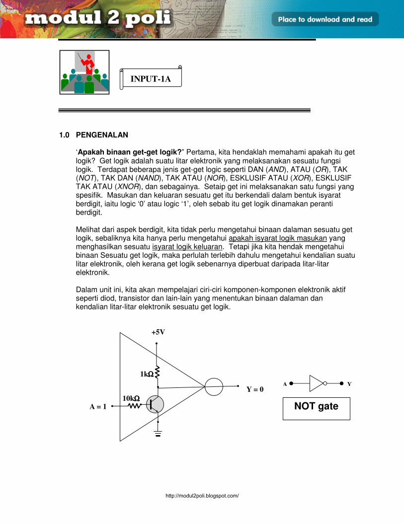
1.0 PENGENALAN
‘Apakah binaan get-get logik?” Pertama, kita hendaklah memahami apakah itu get logik? Get logik adalah suatu litar elektronik yang melaksanakan sesuatu fungsi logik. Terdapat beberapa jenis get-get logic seperti DAN (AND), ATAU (OR), TAK (NOT), TAK DAN (NAND), TAK ATAU (NOR), ESKLUSIF ATAU (XOR), ESKLUSIF TAK ATAU (XNOR), dan sebagainya. Setaip get ini melaksanakan satu fungsi yang spesifik. Masukan dan keluaran sesuatu get itu berkendali dalam bentuk isyarat berdigit, iaitu logic ‘0’ atau logic ‘1’, oleh sebab itu get logik dinamakan peranti berdigit. Melihat dari aspek berdigit, kita tidak perlu mengetahui binaan dalaman sesuatu get logik, sebaliknya kita hanya perlu mengetahui apakah isyarat logik masukan yang menghasilkan sesuatu isyarat logik keluaran. Tetapi jika kita hendak mengetahui binaan Sesuatu get logik, maka perlulah terlebih dahulu mengetahui kendalian suatu litar elektronik, oleh kerana get logik sebenarnya diperbuat daripada litar-litar elektronik. Dalam unit ini, kita akan mempelajari ciri-ciri komponen-komponen elektronik aktif seperti diod, transistor dan lain-lain yang menentukan binaan dalaman dan kendalian litar-litar elektronik sesuatu get logik.
INPUT-1A
Y = 0
+5V
A = 1 10kΩΩΩΩ
1kΩΩΩΩ
NOT gate
A Y
http://modul2poli.blogspot.com/
E3165 / UNIT 1 / 3
PEMBINAAN GET LOGIK ASAS
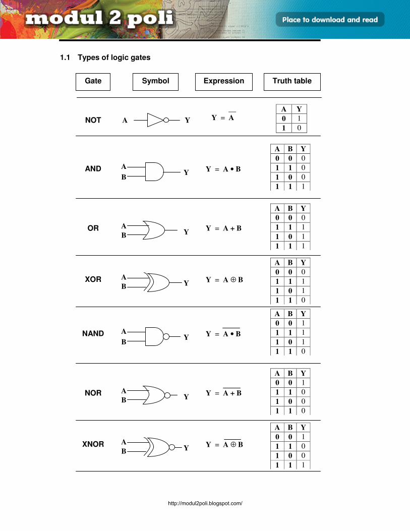
1.1 Types of logic gates
__
Y = A A Y NOT
Gate Symbol Truth table Expression
A Y
0 1
1 0
Y = A • B A
B Y
AND
A B Y
0 0 0
1 1 0
1 0 0
1 1 1
Y = A + B OR
A B Y
0 0 0
1 1 1
1 0 1
1 1 1
A
B Y
Y = A ⊕ B XOR
A B Y
0 0 0
1 1 1
1 0 1
1 1 0
A
B Y
NAND
A B Y
0 0 1
1 1 1
1 0 1
1 1 0
NOR
A B Y
0 0 1
1 1 0
1 0 0
1 1 0
XNOR
A B Y
0 0 1
1 1 0
1 0 0
1 1 1
A
B Y
A
B Y
A
B Y
Y = A • B
Y = A + B
Y = A ⊕ B
http://modul2poli.blogspot.com/
E3165 / UNIT 1 / 4
PEMBINAAN GET LOGIK ASAS
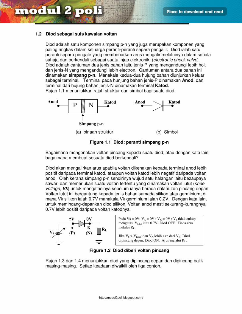
1.2 Diod sebagai suis kawalan voltan
Diod adalah satu komponen simpang p-n yang juga merupakan komponen yang paling ringkas dalam keluarga peranti-peranti separa pengalir. Diod ialah satu peranti separa pengalir yang membenarkan arus mengalir melaluinya dalam sehala sahaja dan berkendali sebagai suatu injap elektronik. (electronic check valve). Diod adalah cantuman dua jenis bahan iaitu jenis-P yang mengandungi lebih hol, dan jenis-N yang mengandungi lebih electron. Cantuman antara dua bahan ini dinamakan simpang p-n. Manakala kedua-dua hujung bahan diunjurkan keluar sebagai terminal. Terminal pada hunjung bahan jenis-P dinamakan Anod, dan terminal dari hujung bahan jenis-N dinamakan terminal Katod. Rajah 1.1 menunjukkan rajah struktur dan simbol bagi suatu diod.
(a) binaan struktur (b) Simbol
Figure 1.1 Diod: peranti simpang p-n Bagaimana mengenakan voltan pincang kepada suatu diod; atau dengan kata lain, bagaimana membuat sesuatu diod berkendali? Diod akan mengalirkan arus apabila voltan dikenakan kepada terminal anod lebih positif daripada terminal katod, ataupun voltan katod lebih negatif daripada voltan anod. Oleh kerana simpang p-n sendirinya wujud satu halangan iaitu bezaupaya sawar, dan memerlukan suatu voltan tertentu yang dinamakan voltan lutut (knee voltage, Vk) untuk mengatasinya sebelum ianya berada dalam zon pincang depan. Voltan lutut ini bergantung kepada jenis bahan samada silikon atau germinium; di mana Vk silikon ialah 0.7V manakala Vk germinium ialah 0.2V. Dengan kata lain, untuk memincang-depankan diod silikon, Voltan anod mesti sekurang-kurangnya 0.7V lebih positif daripada voltan katodnya.
Figure 1.2 Diod diberi voltan pincang Rajah 1.3 dan 1.4 menunjukkan diod yang dipincang depan dan dipincang balik masing-masing. Setiap keadaan diwaikili oleh tiga contoh.
P N Anod Katod
Simpang p-n
Anod Katod
?V 0V
RL A
(P) VS
Pada Vs = 0V; VA = 0V ; VK = 0V ; VS tidak cukup
mengatasi Vlutut iaitu 0.7V; Diod OFF. Tiada arus
melalui RL.
Jika VS > Vlutut; dan VA lebih +ve dari VK; Diod
dipincang depan; Diod ON. Arus melalui RL.
K
(N)
http://modul2poli.blogspot.com/
E3165 / UNIT 1 / 5
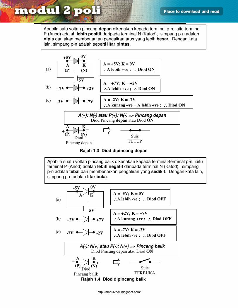
PEMBINAAN GET LOGIK ASAS
Apabila satu voltan pincang depan dikenakan kepada terminal p-n, iaitu terminal P (Anod) adalah lebih positif daripada terminal N (Katod), simpang p-n adalah nipis dan akan membenarkan pengaliran arus yang lebih besar. Dengan kata lain, simpang p-n adalah seperti litar pintas.
Apabila suatu voltan pincang balik dikenakan kepada terminal-terminal p-n, iaitu terminal P (Anod) adalah lebih negatif daripada terminal N (Katod), simpang p-n adalah tebal dan membenarkan pengaliran yang sedikit. Dengan kata lain, simpang p-n adalah litar buka.
+5V 0V
5V
+7V +2V
A = +5V; K = 0V
∴∴∴∴A lebih +ve ; ∴∴∴∴ Diod ON
-2V -7V
A(+): N(-) atau P(+): N(-) => Pincang depan
Diod Pincang depan atau Diod ON
(a)
(b)
(c)
-5V 0V
5V
+2V +7V
A K
-7V -2V
(a)
(b)
(c)
Rajah 1.4 Diod dipincang balik
Rajah 1.3 Diod dipincang depan
A = +7V; K = +2V
∴∴∴∴A lebih +ve ; ∴∴∴∴ Diod ON
A = -2V; K = -7V
∴∴∴∴A kurang –ve = A lebih +ve ; ∴∴∴∴ Diod ON
A = -5V; K = 0V
∴∴∴∴A lebih -ve ; ∴∴∴∴ Diod OFF
A = +2V; K = +7V
∴∴∴∴A kurang +ve ; ∴∴∴∴ Diod OFF
A = -7V; K = -2V
∴∴∴∴A lebih -ve ; ∴∴∴∴ Diod OFF
A(-): N(+) atau P(-): N(+) => Pincang balik
Diod Pincang depan atau Diod ON
A
(P)
K
(N)
+ _
Suis
TUTUP Diod
Pincang depan
A
(P)
K
(N)
_
+
Suis
TERBUKA Diod
Pincang balik
A
(P)
K
(N)
http://modul2poli.blogspot.com/
E3165 / UNIT 1 / 6
PEMBINAAN GET LOGIK ASAS
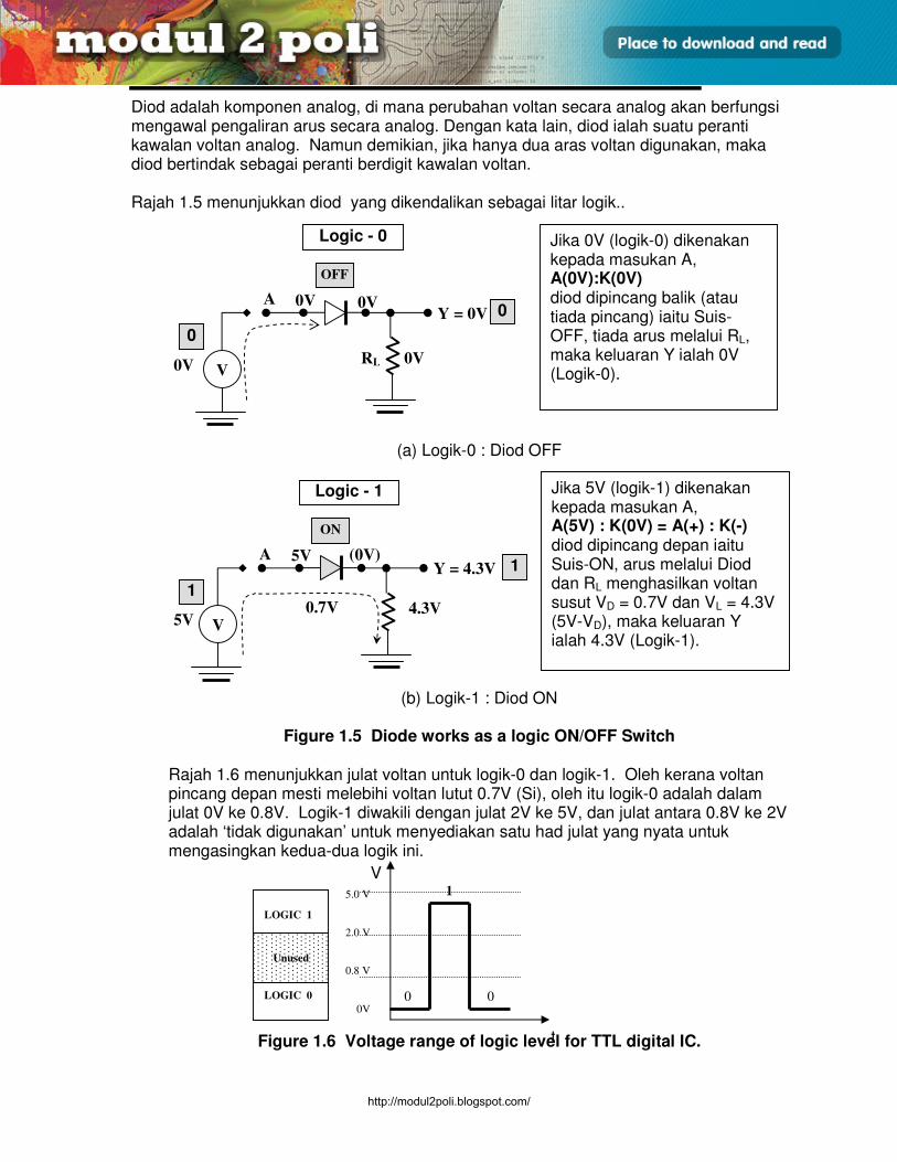
Diod adalah komponen analog, di mana perubahan voltan secara analog akan berfungsi mengawal pengaliran arus secara analog. Dengan kata lain, diod ialah suatu peranti kawalan voltan analog. Namun demikian, jika hanya dua aras voltan digunakan, maka diod bertindak sebagai peranti berdigit kawalan voltan. Rajah 1.5 menunjukkan diod yang dikendalikan sebagai litar logik..
(a) Logik-0 : Diod OFF
(b) Logik-1 : Diod ON
Figure 1.5 Diode works as a logic ON/OFF Switch Rajah 1.6 menunjukkan julat voltan untuk logik-0 dan logik-1. Oleh kerana voltan pincang depan mesti melebihi voltan lutut 0.7V (Si), oleh itu logik-0 adalah dalam julat 0V ke 0.8V. Logik-1 diwakili dengan julat 2V ke 5V, dan julat antara 0.8V ke 2V adalah ‘tidak digunakan’ untuk menyediakan satu had julat yang nyata untuk mengasingkan kedua-dua logik ini.
Figure 1.6 Voltage range of logic level for TTL digital IC.
A 0V
V 0V
Y = 0V
OFF
0V
0V
Logic - 0
0
0
A 5V
V
Y = 4.3V
ON
0.7V 4.3V
Logic - 1
(0V)
1
1
5V
Jika 0V (logik-0) dikenakan kepada masukan A, A(0V):K(0V) diod dipincang balik (atau tiada pincang) iaitu Suis-OFF, tiada arus melalui RL, maka keluaran Y ialah 0V (Logik-0).
LOGIC 1
LOGIC 0
Unused
5.0 V
2.0 V
0.8 V
0V 0 0
1
V
t
RL
Jika 5V (logik-1) dikenakan kepada masukan A, A(5V) : K(0V) = A(+) : K(-) diod dipincang depan iaitu Suis-ON, arus melalui Diod dan RL menghasilkan voltan susut VD = 0.7V dan VL = 4.3V (5V-VD), maka keluaran Y ialah 4.3V (Logik-1).
http://modul2poli.blogspot.com/
E3165 / UNIT 1 / 7
PEMBINAAN GET LOGIK ASAS
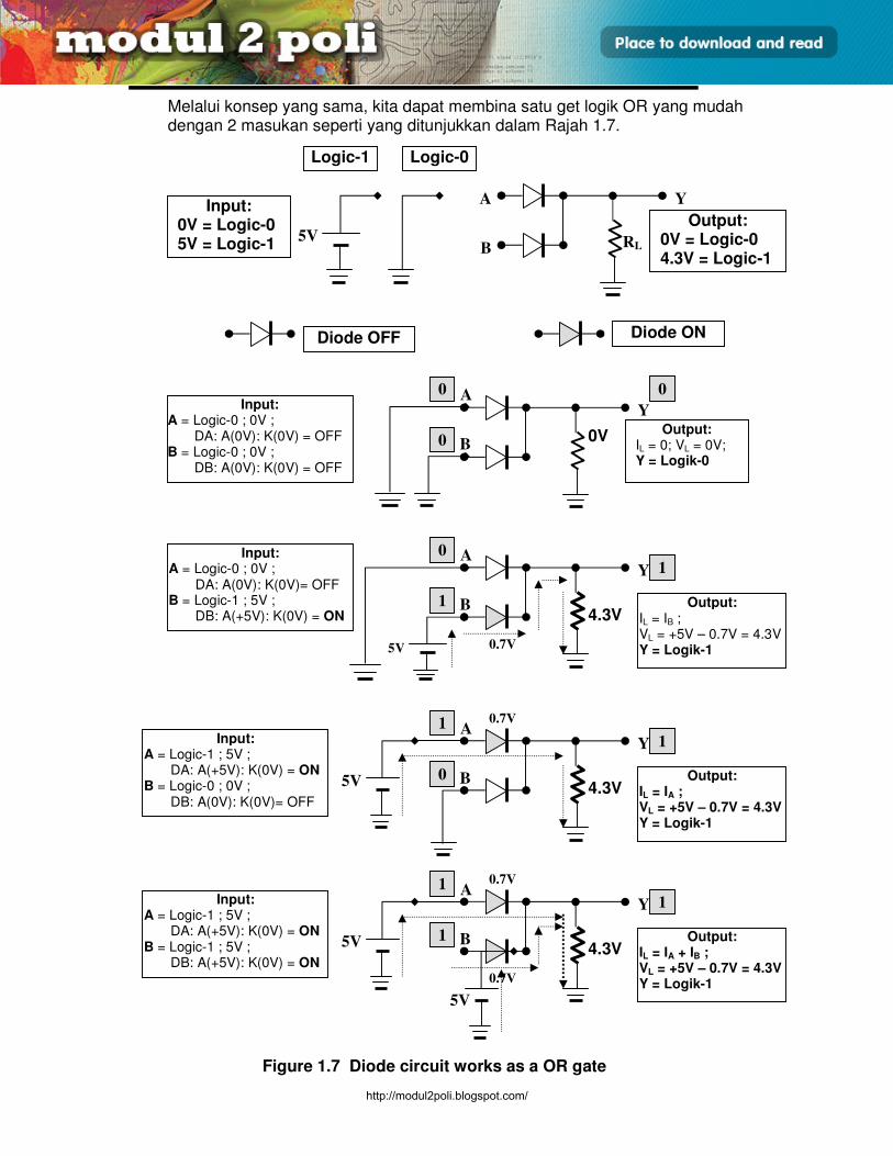
Melalui konsep yang sama, kita dapat membina satu get logik OR yang mudah dengan 2 masukan seperti yang ditunjukkan dalam Rajah 1.7.
Logic-1
5V
A
B
Y
Logic-0
Output: 0V = Logic-0 4.3V = Logic-1
Input: 0V = Logic-0 5V = Logic-1
Input: A = Logic-0 ; 0V ; DA: A(0V): K(0V) = OFF B = Logic-0 ; 0V ; DB: A(0V): K(0V) = OFF
A
B
Y
0V
0
0
0
A
B
Y
4.3V
0
1
1
Diode OFF Diode ON
5V
A
B
Y
4.3V
1
0
1
5V
A
B
Y
4.3V
1
1
1
5V
5V
Figure 1.7 Diode circuit works as a OR gate
0.7V
0.7V
0.7V
0.7V
RL
Input: A = Logic-0 ; 0V ; DA: A(0V): K(0V)= OFF B = Logic-1 ; 5V ; DB: A(+5V): K(0V) = ON
Output: IL = 0; VL = 0V; Y = Logik-0
Output: IL = IB ; VL = +5V – 0.7V = 4.3V Y = Logik-1
Input: A = Logic-1 ; 5V ; DA: A(+5V): K(0V) = ON B = Logic-0 ; 0V ; DB: A(0V): K(0V)= OFF
Output: IL = IA ; VL = +5V – 0.7V = 4.3V Y = Logik-1
Input: A = Logic-1 ; 5V ; DA: A(+5V): K(0V) = ON B = Logic-1 ; 5V ; DB: A(+5V): K(0V) = ON
Output: IL = IA + IB ; VL = +5V – 0.7V = 4.3V Y = Logik-1
http://modul2poli.blogspot.com/
E3165 / UNIT 1 / 8
PEMBINAAN GET LOGIK ASAS
Perbincangan di atas menerangkan bahawa diod secara amnya ialah satu suis kawalan voltan (voltage-controlled switch), dan ianya berkendali sebagai suis-suis logik digit dalam get-get logik. Dengan kata lain, gabungan diod-diod boleh digunakan untuk membina get-get logik.
Input Output A B Y 0 0 0 0 1 1 1 0 1 1 1 1
Dengan menggabungkan keempat-empat keadaan di atas, kita dapat membina satu jadual kebenaran untuk get logik OR. Ini membuiktikan litar elektronik diod melaksanakan fungsi digit sebagai satu get logik (OR)
http://modul2poli.blogspot.com/
E3165 / UNIT 1 / 9
PEMBINAAN GET LOGIK ASAS
1.3 Transistor sebagai suis kawalan voltan.
Satu lagi jenis separa pengalir simpang p-n yang boleh digunakan sebagai suis kawalan voltan ialah transistor. Transistor selalunya dikaitkan sebagai penguat, tetapi dalam kendalian tertentu ia bertindak sebagai suis.
Dalam Rajah 1.3-1, kendalian litar transistor adalah dalam bentuk analog. Jika VBE dikawal pada dua aras voltan sahaja, maka litar transistor ini akan berkendali secara berdigit. Rajah 1.3-2 dan 1.3-3 menunjukkan kedua-dua keadaan suis transistor.
INPUT-1B
Y =VCE
= VCC – VL
VCC
IBE
VL = ICE x RL RL
VBEICE
VBE sebagai bekalan kuasa memincangkan simpang B-
E, lalu mengawal arus IBE.
Manakala IBE akan mengawal ICE iaitu arus melalui
simpang C dan E. Semakin besar IBE, semakin besar ICE.
Jika RL ialah beban, semkin besar ICE semakin besar VL.
Jika terminal Y sebagai keluaran, VY = VCE = VCC - VL.
Di mana VCE berkadar songsang dengan VL atau ICE.
Kesimpulannya; dengan mengawal VBE (masukan),
ICE atau voltan keluaran VY (keluaran) dapat
dikawal. Biasanya VBE yang sangat kecil diperlukan untuk
mengawal ICE yang dibekalkan oleh VCC (yang lebih
besar berbanding VBE). Untuk memulakan kendalian
transistor, VBE mesti lebih besar dariVlutut transistor iaitu
0.7V Si dan 0.3V Ge.
Oleh itu, VBE sebagai isyarat kawalan (sebagai suis)
yang mengawal litar utama VCC.
Dengan kata lain, transistor ini bertindak sebagai
penguat kawalan voltan (VBE).
Rajah 1.3-1 Kendalian litar Transistors
Y =VCC
Logik-1
VCC
IBE = 0
RL
VBE = 0V
Logik-0 ICE = 0
VBE = 0V
Y=VCE
=VCC
VCC
CE terbuka Suis CE
terbuka
Rajah 1.3-2 Transistor dalam keadaan Suis OFF
http://modul2poli.blogspot.com/
E3165 / UNIT 1 / 10
PEMBINAAN GET LOGIK ASAS
Untuk aplikasi logik, pincang depan bagi B-E ditetapkan pada satu nilai tertentu yang hanya berfungsi untuk menyuis transistor pada dua keadaan iaitu logik-0 (lebih kurang 0V), dan logik-1 (lebih kurang 5V). Rajah 1.3-4 menunjukkan satu litar transistor yang berkendali sebagai satu suis digit; dalam kes ini, suatu get NOT.
Figure 1.3-4 Transistor circuit works as a NOT gate.
Y =VCE = 0.2V
(Logik-0)
VCC
IBE
VL = VCC - VCE RL
VBE = +5V
Logik-1
ICE tepu
Rajah 1.3-3 Transistor dalam keadaan Suis ON
CE hampir terpintas,
VCE≈ 0.2V VBE wujud
(Logik-1)
Suis CE
tertutup
Y =VCE
≈ bumi
(Logik-0)
VCC
Tr Saturated
ICE flows,
CE ≈ shorted
VCE ≈ 0.2V
ON
Y =Logic-0
VY = VCE = 0.2V
+5V
A
+5V
Logic-1
A Y 1 0
10kΩΩΩΩ
1kΩΩΩΩ
Bila masukan A dibekalkan satu voltan +5V (Logik-1), VB=+5V dan VE=0V, oleh itu VBE= VB-VE = +5V iaitu simpang B-E dipincang depan, oleh itu transistor dalam keadaan
“saturation” (ON). (Perintang 10kΩ berfungsi sebagai penghad arus, anggapkan voltan susut merentasinya diabaikan). Arus yang sangat besar akan mengalir melalui dari collector ke emitter. Terminal CE seperti dalam litar pintas, dan VCE lebih kurang 0.2V, yang juga sebagai voltan keluaran pada Y (Logik-0). Dengan kata lain, masukan logik-1 akan menghasilkan keluaran logik-0.
0V
+5V
A
Y =Logic-1
0V
Logic-0 0V OFF
Tr Cutoff
No ICE flows,
CE ≈ opened
VCE = Vsupply
= +5V
VY = VCE = +5V A Y 0 1
10kΩΩΩΩ
1kΩΩΩΩ
Bila masukan-A dibekalkan satu voltan 0V (logik-0), VB=0V dan VE=0V, oleh itu VBE= VB-VE = 0V iaitu simpang B-E dipincang balik (belum dipincang depan), oleh itu transistor dalam keadaan “cutoff” (OFF). Tiada arus mengalir melalui dari collector ke emitter. Terminal CE litar-buka, dan VCE adalah menghampiri voltan bekalan, i.e +5V, yang juga sebagai voltan keluaran pada Y (logik-1). Dengan kata lain, masukan logik-0 akan menghasilkan keluaran logik-1.
VBE = 5V- 0V = 5V
BE pincang depan
http://modul2poli.blogspot.com/
E3165 / UNIT 1 / 11
PEMBINAAN GET LOGIK ASAS
Nota tambahan:
Transistor pada keadaan suis OFF
• Perintang disambungkan antara pemungut dan bekalan +5V bagi menghasilkan arus pemungut, Ic.
• Apabila arus tapak sifar (Ib = 0), arus pemancar Ie dan Ic juga sifar (abaikan arus bocor).
• Transistor berada dalam keadaan cut-off.
• Dalam suis elektrik ia dianggap dalam keadaan terbuka (suis buka) antara pemungut dan pemancar.
• Tiada voltan dihasilkan merintangi perintang kerana tiada arus melalui perintang (Hukum Ohm, V = IR).
• Voltan keluaran pada pemungut adalah sama dengan voltan bekalan iaitu 5V.
• Keadaan cut-off ini boleh dicapai dengan memberikan 0V antara tapak dan pemancar (Vbe = 0) tetapi voltan < 0.6V (voltan lutut) adalah mencukupi.
Transistor pada keadaan suis ON
• Apabila Vbe > 0.6V dikenakan, arus tapak (Ib) akan meningkat dan Ic juga meningkat (Ic = Bib).
• Voltan merintangi perintang akan meningkat (V=IR) dan Vce akan menurun.
• Voltan minima pemungut-pemancar dikenali sebagai voltan tepu, Vce-sat = 0.2V.
• Jika arus tapak terus meningkat, Bib > Ic dan transistor dikatakan dalam keadaan tepu.
• Dalam keadaan tepu, transistor dianggap sebagai suis tutup dan dalam keadaan ON.
• Dianggapkan Vbe = 0.7V adalah mencukupi untuk menghasilkan keadaan tepu bagi transistor.
http://modul2poli.blogspot.com/
E3165 / UNIT 1 / 12
PEMBINAAN GET LOGIK ASAS
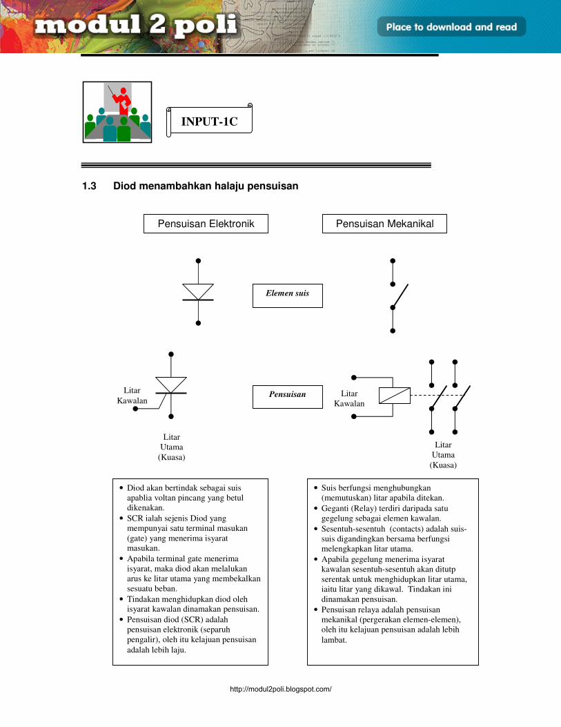
1.3 Diod menambahkan halaju pensuisan
INPUT-1C
Pensuisan Elektronik
Litar
Kawalan
Litar
Utama
(Kuasa)
Pensuisan Mekanikal
Litar
Kawalan
Litar
Utama
(Kuasa)
• Diod akan bertindak sebagai suis
apablia voltan pincang yang betul
dikenakan.
• SCR ialah sejenis Diod yang
mempunyai satu terminal masukan
(gate) yang menerima isyarat
masukan.
• Apabila terminal gate menerima
isyarat, maka diod akan melalukan
arus ke litar utama yang membekalkan
sesuatu beban.
• Tindakan menghidupkan diod oleh
isyarat kawalan dinamakan pensuisan.
• Pensuisan diod (SCR) adalah
pensuisan elektronik (separuh
pengalir), oleh itu kelajuan pensuisan
adalah lebih laju.
• Suis berfungsi menghubungkan
(memutuskan) litar apabila ditekan.
• Geganti (Relay) terdiri daripada satu
gegelung sebagai elemen kawalan.
• Sesentuh-sesentuh (contacts) adalah suis-
suis digandingkan bersama berfungsi
melengkapkan litar utama.
• Apabila gegelung menerima isyarat
kawalan sesentuh-sesentuh akan ditutp
serentak untuk menghidupkan litar utama,
iaitu litar yang dikawal. Tindakan ini
dinamakan pensuisan.
• Pensuisan relaya adalah pensuisan
mekanikal (pergerakan elemen-elemen),
oleh itu kelajuan pensuisan adalah lebih
lambat.
Elemen suis
Pensuisan
http://modul2poli.blogspot.com/
E3165 / UNIT 1 / 13
PEMBINAAN GET LOGIK ASAS
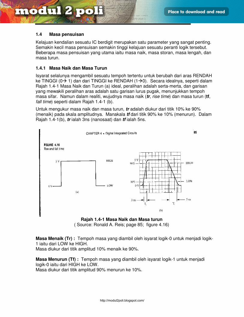
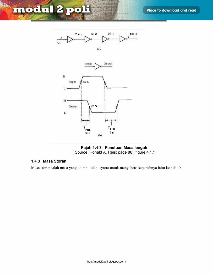
1.4 Masa pensuisan
Kelajuan kendalian sesuatu IC berdigit merupakan satu parameter yang sangat penting. Semakin kecil masa pensuisan semakin tinggi kelajuan sesuatu peranti logik tersebut. Beberapa masa pensuisan yang utama iaitu masa naik, masa storan, masa lengah, dan masa turun. 1.4.1 Masa Naik dan Masa Turun
Isyarat selalunya mengambil sesuatu tempoh tertentu untuk berubah dari aras RENDAH ke TINGGI (0 1) dan dari TINGGI ke RENDAH (10). Secara idealnya, seperti dalam Rajah 1.4-1 Masa Naik dan Turun (a) ideal, peralihan adalah serta-merta, dan garisan yang mewakili peralihan aras adalah satu garisan lurus pugak, menunjukkan tempoh masa sifar. Namun dalam realiti, wujudnya masa naik (tr, rise time) dan masa turun (tf, fall time) seperti dalam Rajah 1.4-1 (b).
Untuk mengukur masa naik dan masa turun, tr adalah diukur dari titik 10% ke 90% (menaik) pada skala amplitudnya. Manakala tf dari titik 90% ke 10% (menurun). Dalam Rajah 1.4-1(b), tr ialah 3ns (nanosaat) dan tf ialah 5ns.
Masa Menaik (Tr) : Tempoh masa yang diambil oleh isyarat logik-0 untuk menjadi logik-1 iaitu dari LOW ke HIGH. Masa diukur dari titik amplitud 10% menaik ke 90%. Masa Menurun (Tf) : Tempoh masa yang diambil oleh isyarat logik-1 untuk menjadi logik-0 iaitu dari HIGH ke LOW. Masa diukur dari titik amplitud 90% menurun ke 10%.
ideal real
Rajah 1.4-1 Masa Naik dan Masa turun ( Source: Ronald A. Reis; page 85; figure 4.16)
http://modul2poli.blogspot.com/
E3165 / UNIT 1 / 14
PEMBINAAN GET LOGIK ASAS
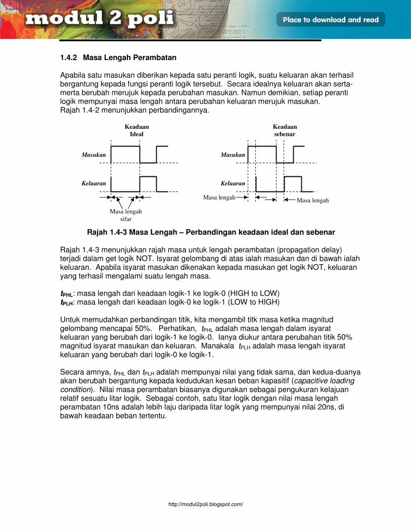
1.4.2 Masa Lengah Perambatan Apabila satu masukan diberikan kepada satu peranti logik, suatu keluaran akan terhasil bergantung kepada fungsi peranti logik tersebut. Secara idealnya keluaran akan serta-merta berubah merujuk kepada perubahan masukan. Namun demikian, setiap peranti logik mempunyai masa lengah antara perubahan keluaran merujuk masukan. Rajah 1.4-2 menunjukkan perbandingannya.
Rajah 1.4-3 Masa Lengah – Perbandingan keadaan ideal dan sebenar Rajah 1.4-3 menunjukkan rajah masa untuk lengah perambatan (propagation delay) terjadi dalam get logik NOT. Isyarat gelombang di atas ialah masukan dan di bawah ialah keluaran. Apabila isyarat masukan dikenakan kepada masukan get logik NOT, keluaran yang terhasil mengalami suatu lengah masa. tPHL: masa lengah dari keadaan logik-1 ke logik-0 (HIGH to LOW) tPLH: masa lengah dari keadaan logik-0 ke logik-1 (LOW to HIGH) Untuk memudahkan perbandingan titik, kita mengambil titk masa ketika magnitud gelombang mencapai 50%. Perhatikan, tPHL adalah masa lengah dalam isyarat keluaran yang berubah dari logik-1 ke logik-0. Ianya diukur antara perubahan titik 50% magnitud isyarat masukan dan keluaran. Manakala tPLH adalah masa lengah isyarat keluaran yang berubah dari logik-0 ke logik-1. Secara amnya, tPHL dan tPLH adalah mempunyai nilai yang tidak sama, dan kedua-duanya akan berubah bergantung kepada kedudukan kesan beban kapasitif (capacitive loading condition). Nilai masa perambatan biasanya digunakan sebagai pengukuran kelajuan relatif sesuatu litar logik. Sebagai contoh, satu litar logik dengan nilai masa lengah perambatan 10ns adalah lebih laju daripada litar logik yang mempunyai nilai 20ns, di bawah keadaan beban tertentu.
Masa lengah Masa lengah
Masa lengah
sifar
Keadaan
Ideal
Keadaan
sebenar
Masukan
Keluaran
Masukan
Keluaran
http://modul2poli.blogspot.com/
E3165 / UNIT 1 / 15
PEMBINAAN GET LOGIK ASAS
Rajah 1.4-3 Penetuan Masa lengah ( Source: Ronald A. Reis; page 86; figure 4.17)
1.4.3 Masa Storan
Masa storan ialah masa yang diambil oleh isyarat untuk menyahcas sepenuhnya iaitu ke nilai 0.
http://modul2poli.blogspot.com/
E3165 / UNIT 1 / 16
PEMBINAAN GET LOGIK ASAS
1.5 Famili TTL
Dalam aspek pembuatan komponen, beberapa get logik yang sama jenis digabungkan dalam satu cip, yang dinamakan litar bersepadu atau singkatan IC (integrated circuit) dan dilabelkan dengan suatu nombor tertentu, seperti 7400 ialah get NAND, 7404 ialah get NOT. Dua famili IC yang umum yang banyak digunakan kini ialah TTL (Transistor-Transistor Logic) dan CMOS (Complementary Metal-Oxide Semiconductor).
TTL Series: 74 Series: First line of standard TTL ICs. 74L and 74H Series: developed to provide low-power and high-speed versions of TTL respectively. 74S Series: Schottky TTL, reduces storage time delay by not allowing the transistor to go as deeply into saturation, which is encountered in the 74, 74H, 74L series. 74LS Series: Low-Power Schottky TTL. 74AS Series: Advanced Schottky TTL. 74ALS Series: Advanced Low-Power Schottky TTL. 74F Series: Fast TTL
Perbezaan yang utama antara versi 54 dan 74 ialah peranti versi 54 berupaya berkendali dalam satu julat yang lebih besar terhadap suhu dan voltan bekalan kuasa. Oleh itu IC 5400 dan 7400 ialah IC get logic (NAND) yang sama. IC siri 54 biasanya digunakan dalam keadaan yang lebih lasak seperti kegunaan militari.
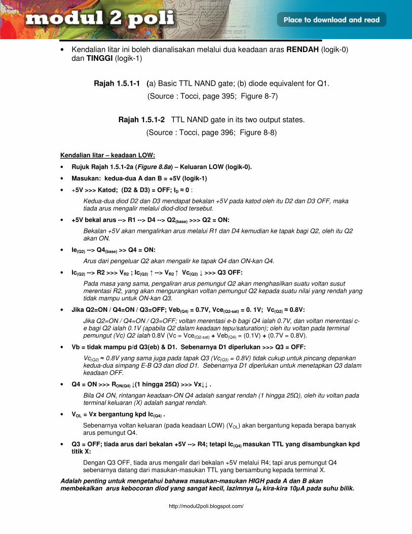
1.5.1 TTL NAND Gate Operation
• Litar logic asas TTL ialah get TAKDAN (NAND), oleh itu kita menganalisa litar elektronik bagi TTL dalam get NAND, seperti yang ditunjukkan dalam Rajah 1.5.1-1 Basic TTL NAND gate (Tocci, Fig 8-7, pg 395).
• Litar ini mempunyai beberapa ciri yang istimewa. Pertamanya, perhatikan transistor Q1 yang mempunyai dua terminal pengeluar; oleh itu ianya mempunyai dua simpang tapak-pengeluar (b-e) yang boleh menghidupkan Q1. Transistor dengan masukan pelbagai-pengeluar boleh memiliki sehingga 8 terminal pengeluar untuk membentuk satu get NAND 8 masukan.
• Transistor pelbagai-pengeluar (multiple-emmitter) ini (Q1) sebenarnya boleh diwakili oleh satu litar mudah seperti dalam Rajah 1.5.1-1 (b). Diod D2 dan D3 mewakili dua simpang b-e bagi Q1, dan D4 ialah simpang pemungut-tapak (C-B). Litar perwakilan ini akan digunakan dalam penerangan berikutnya.
• Juga diperhatikan pada keluaran litar, transistor Q3 dan Q4 adalah dalam susunatur tiang elu (Totem Pole). Dalam keadaan kendalian yang normal, salah satu transistor Q3 atau Q4 akan hidup, bergantung kepada aras logic bagi keluaran.
INPUT-1D
http://modul2poli.blogspot.com/
E3165 / UNIT 1 / 17
PEMBINAAN GET LOGIK ASAS
• Kendalian litar ini boleh dianalisakan melalui dua keadaan aras RENDAH (logik-0) dan TINGGI (logik-1)
Rajah 1.5.1-1 (a) Basic TTL NAND gate; (b) diode equivalent for Q1.
(Source : Tocci, page 395; Figure 8-7)
Rajah 1.5.1-2 TTL NAND gate in its two output states.
(Source : Tocci, page 396; Figure 8-8)
Kendalian litar – keadaan LOW:
• Rujuk Rajah 1.5.1-2a (Figure 8.8a) – Keluaran LOW (logik-0).
• Masukan: kedua-dua A dan B = +5V (logik-1)
• +5V >>> Katod; (D2 & D3) = OFF; ID ≈ 0 :
Kedua-dua diod D2 dan D3 mendapat bekalan +5V pada katod oleh itu D2 dan D3 OFF, maka tiada arus mengalir melalui diod-diod tersebut.
• +5V bekal arus --> R1 --> D4 --> Q2(base) >>> Q2 = ON:
Bekalan +5V akan mengalirkan arus melalui R1 dan D4 kemudian ke tapak bagi Q2, oleh itu Q2 akan ON.
• Ie(Q2) --> Q4(base) >> Q4 = ON:
Arus dari pengeluar Q2 akan mengalir ke tapak Q4 dan ON-kan Q4.
• Ic(Q2) --> R2 >>> VR2 ; Ic(Q2) ↑ --> VR2 ↑ Vc(Q2) ↓ >>> Q3 OFF:
Pada masa yang sama, pengaliran arus pemungut Q2 akan menghasilkan suatu voltan susut merentasi R2, yang akan mengurangkan voltan pemungut Q2 kepada suatu nilai yang rendah yang tidak mampu untuk ON-kan Q3.
• Jika Q2=ON / Q4=ON / Q3=OFF; Veb(Q4) = 0.7V, Vce(Q2-sat) = 0. 1V; Vc(Q2) ≈ 0.8V:
Jika Q2=ON / Q4=ON / Q3=OFF; voltan merentasi e-b bagi Q4 ialah 0.7V, dan voltan merentasi c-e bagi Q2 ialah 0.1V (apabila Q2 dalam keadaan tepu/saturation); oleh itu voltan pada terminal pemungut (Vc) Q2 ialah 0.8V (Vc = Vce(Q2-sat) + Veb(Q4) = (0.1V) + (0.7V = 0.8V).
• Vb = tidak mampu p/d Q3(eb) & D1. Sebenarnya D1 diperlukan >>> Q3 = OFF:
Vc(Q2) ≈ 0.8V yang sama juga pada tapak Q3 (Vc(Q3) = 0.8V) tidak cukup untuk pincang depankan kedua-dua simpang E-B Q3 dan diod D1. Sebenarnya D1 diperlukan untuk menetapkan Q3 dalam keadaan OFF.
• Q4 = ON >>> RON(Q4) ↓(1 hingga 25Ω) >>> Vx↓↓ .
Bila Q4 ON, rintangan keadaan-ON Q4 adalah sangat rendah (1 hingga 25Ω), oleh itu voltan pada terminal keluaran (X) adalah sangat rendah.
• VOL = Vx bergantung kpd Ic(Q4) .
Sebenarnya voltan keluaran (pada keadaan LOW) (VOL) akan bergantung kepada berapa banyak arus pemungut Q4.
• Q3 = OFF; tiada arus dari bekalan +5V --> R4; tetapi Ic(Q4) masukan TTL yang disambungkan kpd titik X:
Dengan Q3 OFF, tiada arus mengalir dari bekalan +5V melalui R4; tapi arus pemungut Q4 sebenarnya datang dari masukan-masukan TTL yang bersambung kepada terminal X.
Adalah penting untuk mengetahui bahawa masukan-masukan HIGH pada A dan B akan membekalkan arus kebocoran diod yang sangat kecil, lazimnya IIH kira-kira 10µA pada suhu bilik.
http://modul2poli.blogspot.com/
E3165 / UNIT 1 / 18
PEMBINAAN GET LOGIK ASAS
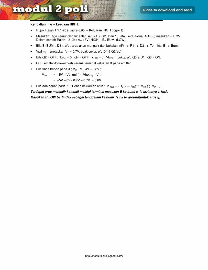
Kendalian litar – keadaan HIGH:
• Rujuk Rajah 1.5.1-2b (Figure 8.8b) – Keluaran HIGH (logik-1).
• Masukan: tiga kemungkinan: salah satu (AB = 01 atau 10) atau kedua-dua (AB=00) masukan = LOW. Dalam contoh Rajah 1.6-2b : A= +5V (HIGH) ; B= BUMI (LOW)
• Bila B=BUMI ; D3 = p/d ; arus akan mengalir dari bekalan +5V --> R1 --> D3 --> Terminal B --> Bumi.
• Vpd(D3) menetapkan VY = 0.7V; tidak cukup p/d D4 & Q2(eb)
• Bila Q2 = OFF; Ib(Q4) = 0 ; Q4 = OFF ; Ic(Q2) = 0 ; Vb(Q3) ↑ cukup p/d Q3 & D1 ; Q3 = ON.
• Q3 = emitter-follower oleh kerana terminal keluaran X pada emitter.
• Bila tiada beban pada X ; VOH ≈ 3.4V – 3.8V ;
VOH = +5V – VR2 (min) – Vbe(Q3) – VD1
= +5V – 0V - 0.7V – 0.7V = 3.6V
• Bila ada beban pada X ; Beban keluarkan arus : Ie(Q3) --> R2 >>> IR2↑ ; VR2 ↑ ; VOH ↓
Terdapat arus mengalir kembali melalui terminal masukan B ke bumi = IIL lazimnya 1.1mA.
Masukan B LOW bertindak sebagai tenggelam ke bumi (sink to ground)untuk arus IIL .
http://modul2poli.blogspot.com/
E3165 / UNIT 1 / 19
PEMBINAAN GET LOGIK ASAS
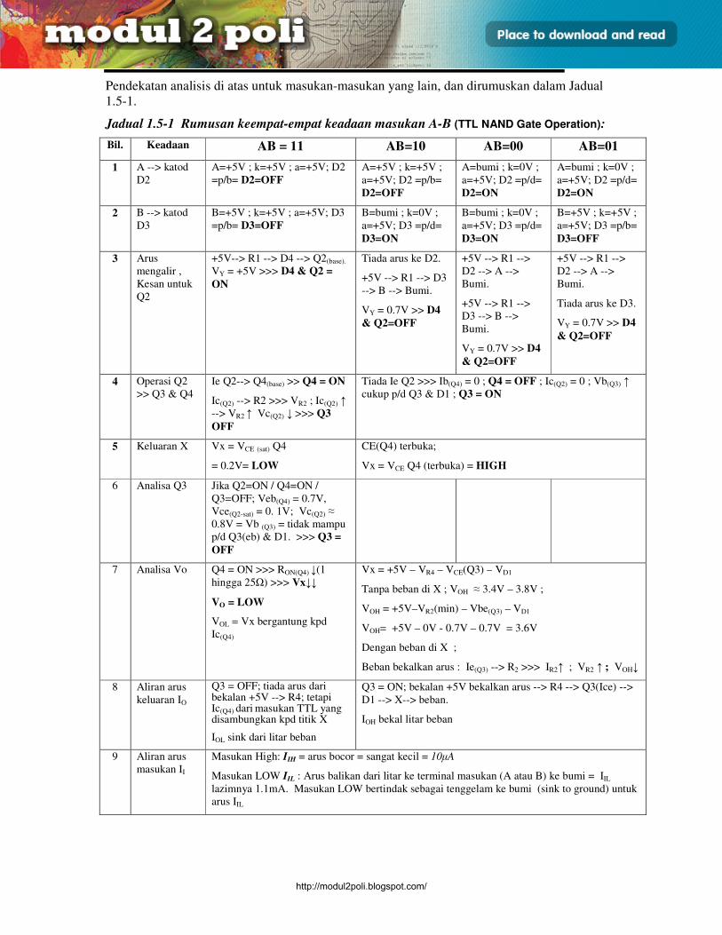
Pendekatan analisis di atas untuk masukan-masukan yang lain, dan dirumuskan dalam Jadual
1.5-1.
Jadual 1.5-1 Rumusan keempat-empat keadaan masukan A-B (TTL NAND Gate Operation):
Bil. Keadaan AB = 11 AB=10 AB=00 AB=01
1 A --> katod
D2
A=+5V ; k=+5V ; a=+5V; D2
=p/b= D2=OFF
A=+5V ; k=+5V ;
a=+5V; D2 =p/b=
D2=OFF
A=bumi ; k=0V ;
a=+5V; D2 =p/d=
D2=ON
A=bumi ; k=0V ;
a=+5V; D2 =p/d=
D2=ON
2 B --> katod
D3
B=+5V ; k=+5V ; a=+5V; D3
=p/b= D3=OFF
B=bumi ; k=0V ;
a=+5V; D3 =p/d=
D3=ON
B=bumi ; k=0V ;
a=+5V; D3 =p/d=
D3=ON
B=+5V ; k=+5V ;
a=+5V; D3 =p/b=
D3=OFF
3 Arus
mengalir ,
Kesan untuk
Q2
+5V--> R1 --> D4 --> Q2(base).
VY = +5V >>> D4 & Q2 =
ON
Tiada arus ke D2.
+5V --> R1 --> D3
--> B --> Bumi.
VY = 0.7V >> D4
& Q2=OFF
+5V --> R1 -->
D2 --> A -->
Bumi.
+5V --> R1 -->
D3 --> B -->
Bumi.
VY = 0.7V >> D4
& Q2=OFF
+5V --> R1 -->
D2 --> A -->
Bumi.
Tiada arus ke D3.
VY = 0.7V >> D4
& Q2=OFF
4 Operasi Q2
>> Q3 & Q4
Ie Q2--> Q4(base) >> Q4 = ON
Ic(Q2) --> R2 >>> VR2 ; Ic(Q2) ↑
--> VR2 ↑ Vc(Q2) ↓ >>> Q3
OFF
Tiada Ie Q2 >>> Ib(Q4) = 0 ; Q4 = OFF ; Ic(Q2) = 0 ; Vb(Q3) ↑ cukup p/d Q3 & D1 ; Q3 = ON
5 Keluaran X Vx = VCE (sat) Q4
= 0.2V= LOW
CE(Q4) terbuka;
Vx = VCE Q4 (terbuka) = HIGH
6 Analisa Q3 Jika Q2=ON / Q4=ON /
Q3=OFF; Veb(Q4) = 0.7V,
Vce(Q2-sat) = 0. 1V; Vc(Q2) ≈
0.8V = Vb (Q3) = tidak mampu
p/d Q3(eb) & D1. >>> Q3 =
OFF
7 Analisa Vo Q4 = ON >>> RON(Q4) ↓(1
hingga 25Ω) >>> Vx↓↓
VO = LOW
VOL = Vx bergantung kpd
Ic(Q4)
Vx = +5V – VR4 – VCE(Q3) – VD1
Tanpa beban di X ; VOH ≈ 3.4V – 3.8V ;
VOH = +5V–VR2(min) – Vbe(Q3) – VD1
VOH= +5V – 0V - 0.7V – 0.7V = 3.6V
Dengan beban di X ;
Beban bekalkan arus : Ie(Q3) --> R2 >>> IR2↑ ; VR2 ↑ ; VOH↓
8 Aliran arus
keluaran IO
Q3 = OFF; tiada arus dari bekalan +5V --> R4; tetapi Ic(Q4) dari masukan TTL yang disambungkan kpd titik X
IOL sink dari litar beban
Q3 = ON; bekalan +5V bekalkan arus --> R4 --> Q3(Ice) -->
D1 --> X--> beban.
IOH bekal litar beban
9 Aliran arus
masukan II
Masukan High: IIH = arus bocor = sangat kecil = 10µA
Masukan LOW IIL : Arus balikan dari litar ke terminal masukan (A atau B) ke bumi = IIL
lazimnya 1.1mA. Masukan LOW bertindak sebagai tenggelam ke bumi (sink to ground) untuk
arus IIL
http://modul2poli.blogspot.com/
E3165 / UNIT 1 / 20
PEMBINAAN GET LOGIK ASAS
1.5.2 Schottky TTL 74S
• IC siri 74L dan 74H ialah versi baru untuk memperbaiki kebolehan siri 74 yang asas.
• Siri 74L ialah versi kuasa rendah (Low-power) yang menggunakan kuasa yang rendah (1mW) tetapi dengan mengalami kelemahan lengah perambatan yang lebih panjang (33ns).
• Siri 74H ialah versi kelajuan tinggi (High-speed) mempunyai lengah perambatan yang kecil (6ns) dengan kos pada penggunaan kuasa yang lebih tinggi (23mW).
• Kesemua siri 74, 74H & 74L berkendali menggunakan pensuisan tepu (saturated switching), di mana banyak transistor, bila berkendali akan berada dalam keadaan tepu.
• Kendalian seumpama ini menyebabkan suatu lengah masa storan (ts) apabila transistor disuis dari ON ke OFF, dan ini akan menghadkan kelajuan pensuisan litar.
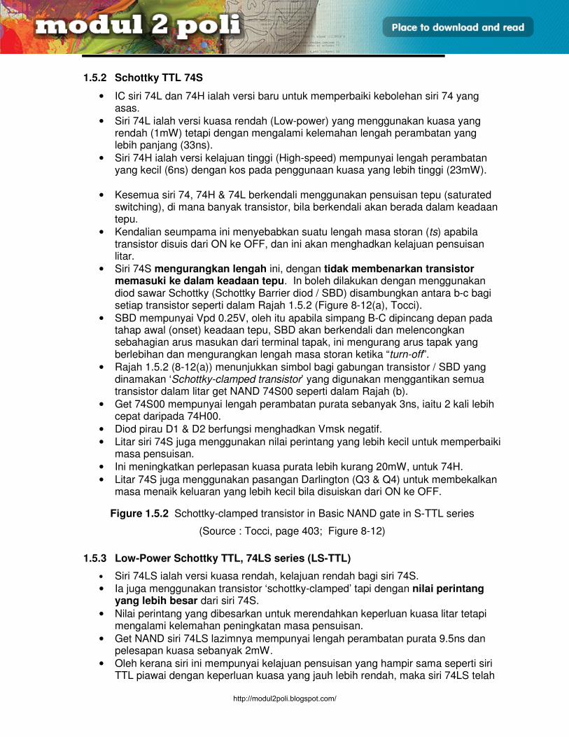
• Siri 74S mengurangkan lengah ini, dengan tidak membenarkan transistor memasuki ke dalam keadaan tepu. In boleh dilakukan dengan menggunakan diod sawar Schottky (Schottky Barrier diod / SBD) disambungkan antara b-c bagi setiap transistor seperti dalam Rajah 1.5.2 (Figure 8-12(a), Tocci).
• SBD mempunyai Vpd 0.25V, oleh itu apabila simpang B-C dipincang depan pada tahap awal (onset) keadaan tepu, SBD akan berkendali dan melencongkan sebahagian arus masukan dari terminal tapak, ini mengurang arus tapak yang berlebihan dan mengurangkan lengah masa storan ketika “turn-off”.
• Rajah 1.5.2 (8-12(a)) menunjukkan simbol bagi gabungan transistor / SBD yang dinamakan ‘Schottky-clamped transistor’ yang digunakan menggantikan semua transistor dalam litar get NAND 74S00 seperti dalam Rajah (b).
• Get 74S00 mempunyai lengah perambatan purata sebanyak 3ns, iaitu 2 kali lebih cepat daripada 74H00.
• Diod pirau D1 & D2 berfungsi menghadkan Vmsk negatif.
• Litar siri 74S juga menggunakan nilai perintang yang lebih kecil untuk memperbaiki masa pensuisan.
• Ini meningkatkan perlepasan kuasa purata lebih kurang 20mW, untuk 74H.
• Litar 74S juga menggunakan pasangan Darlington (Q3 & Q4) untuk membekalkan masa menaik keluaran yang lebih kecil bila disuiskan dari ON ke OFF.
Figure 1.5.2 Schottky-clamped transistor in Basic NAND gate in S-TTL series
(Source : Tocci, page 403; Figure 8-12)
1.5.3 Low-Power Schottky TTL, 74LS series (LS-TTL)
• Siri 74LS ialah versi kuasa rendah, kelajuan rendah bagi siri 74S.
• Ia juga menggunakan transistor ‘schottky-clamped’ tapi dengan nilai perintang yang lebih besar dari siri 74S.
• Nilai perintang yang dibesarkan untuk merendahkan keperluan kuasa litar tetapi mengalami kelemahan peningkatan masa pensuisan.
• Get NAND siri 74LS lazimnya mempunyai lengah perambatan purata 9.5ns dan pelesapan kuasa sebanyak 2mW.
• Oleh kerana siri ini mempunyai kelajuan pensuisan yang hampir sama seperti siri TTL piawai dengan keperluan kuasa yang jauh lebih rendah, maka siri 74LS telah
http://modul2poli.blogspot.com/
E3165 / UNIT 1 / 21
PEMBINAAN GET LOGIK ASAS
menjadi pilihan utama dalam keluarga TTL,dan ianya juga boleh didapati dalam rekabentuk baru yang tidak memerlukan kelajuan maksima.
1.5.4 Advanced Schottky TTL, 74AS Series (AS-TTL)
• Kemajuan selepas siri 74LS ialah siri 74AS yang membekalkan pembaikan dalam aspek kelajuan dengan keperluan kuasa yang lebih kecil.
• Judual 1.5.4-1 (Table 8-4, Tocci) menunjukkan perbandingan siri 74S dan 74AS untuk get NAND terhadap beberapa parameter utama. Ketiga-tiga parameter menunjukkan kelebihan siri 74AS terhadap 74S.
• Siri 74AS juga mempunyai kelebihan iaitu keperluan arus masukan (IIL, IIH) yang lebih rendah, yang memberi rebak-luar (fan-out) yang lebih besar berbanding siri 74S.
• Siri 74ALS ialah Advanced Low-pwer Schottky merupakan penambahbaikan ke atas siri 74LS dalam kedua-dua parameter kelajuan dan pelesapan kuasa seperti yang ditunjukkan dalam Jadual 1.5.4-2 (Table 8-5, Tocci).
Jadual 1.5.4-1 Comparison of TTL series 74S and 74AS
(Source: Ronald J. Tocci; page 404; Table 8-4) 74S 74AS
Propagation Delay 3 ns 1.7 ns
Power Dissipation 20 mW 8mW
Speed-Power Product 60 pJ 13.6pJ
Jadual 1.5.4-2 Comparison of TTL series 74LS and 74ALS
(Source: Ronald J. Tocci; page 404; Table 8-5) 74LS 74ALS
Propagation Delay 9.5 ns 4 ns
Power Dissipation 2 mW 1.2mW
Speed-Power Product 19 pJ 4.8pJ
Jadual 1.5.4-3 (Table 8-6, Tocci) menunjukkan perbandingan beberapa siri 74 terhadap parameter-parameter utama.
Jadual 1.5.4-3 Comparison of TTL 74 series
(Source: Ronald J. Tocci; page 405; Table 8-6)
http://modul2poli.blogspot.com/
E3165 / UNIT 1 / 22
PEMBINAAN GET LOGIK ASAS
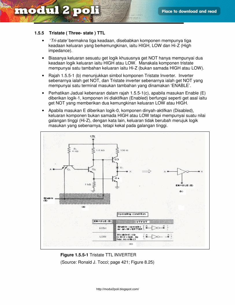
1.5.5 Tristate ( Three- state ) TTL
• ‘Tri-state’ bermakna tiga keadaan, disebabkan komponen mempunya tiga keadaan keluaran yang berkemungkinan, iaitu HIGH, LOW dan Hi-Z (High impedance).
• Biasanya keluaran sesuatu get logik khususnya get NOT hanya mempunyai dua keadaan logik keluaran iaitu HIGH atau LOW. Manakala komponen tristate mempunyai satu tambahan keluaran iaitu Hi-Z (bukan samada HIGH atau LOW).
• Rajah 1.5.5-1 (b) menunjukkan simbol komponen Tristate Inverter. Inverter sebenarnya ialah get NOT, dan Tristate inverter sebenarnya ialah get NOT yang mempunyai satu terminal masukan tambahan yang dinamakan ‘ENABLE’.
• Perhatikan Jadual kebenaran dalam rajah 1.5.5-1(c), apabila masukan Enable (E) diberikan logik-1, komponen ini diaktifkan (Enabled) berfungsi seperti get asal iaitu get NOT yang memberikan dua kemungkinan keluaran LOW atau HIGH.
• Apabila masukan E diberikan logik-0, komponen dinyah-aktifkan (Disabled), keluaran komponen bukan samada HIGH atau LOW tetapi mempunyai suatu nilai galangan tinggi (Hi-Z), dengan kata lain, keluaran tidak berubah merujuk logik masukan yang sebenarnya, tetapi kekal pada galangan tinggi.
Figure 1.5.5-1 Tristate TTL INVERTER
(Source: Ronald J. Tocci; page 421; Figure 8.25)
http://modul2poli.blogspot.com/
E3165 / UNIT 1 / 23
PEMBINAAN GET LOGIK ASAS
• Perbincangan di atas hanyalah penganalisaan secara konsep dan berasaskan simbol komponen. Untuk menganalisa secara litar elektronik, Rajah 1.5.5-1(a) perlu dirujuk.
• Litar Tristate Inverter adalah diubahsuai daripada litar get NAND asas TTL dalam Rajah 1.5.1, di mana terminal masukan kedua (B) diubahsuai menjadi terminal ENABLE. Manakala terminal A kekal sebagai terminal masukan biasa.
• Pada keadaan Enable, masukan E = logik-1: litar ini berfungsi sebagai get NOT yang biasa, kerana voltan HIGH pada E tidak mempunyai kesan ke atas Q1 dan D2. Oleh itu keluaran bergantung kepada masukan A sahaja.
• Pada keadaan Disable, masukan E = logik-0: litar ini berada dalam keadaan Hi-Z tidak peduli keadaan masukan A.
• Logik LOW pada E memincang depan simpang e-b Q1 dan memesong arus dari R2 (1.6k) daripada Q2 supaya Q2 di-OFFkan, seterusnya OFFkan Q4.
• Logik LOW pada E juga memincang depan D2 untuk memesong arus ke tapak Q3 supaya Q3 akan OFF.
• Dengan kedua-dua transistor Totem-pole iaitu Q3 dan Q4 dalam keadaan OFF, terminal keluaran adalah dalam litar-buka, ini ditunjukkan pada simbol dalam Rajah 1.5.5-1 (c).
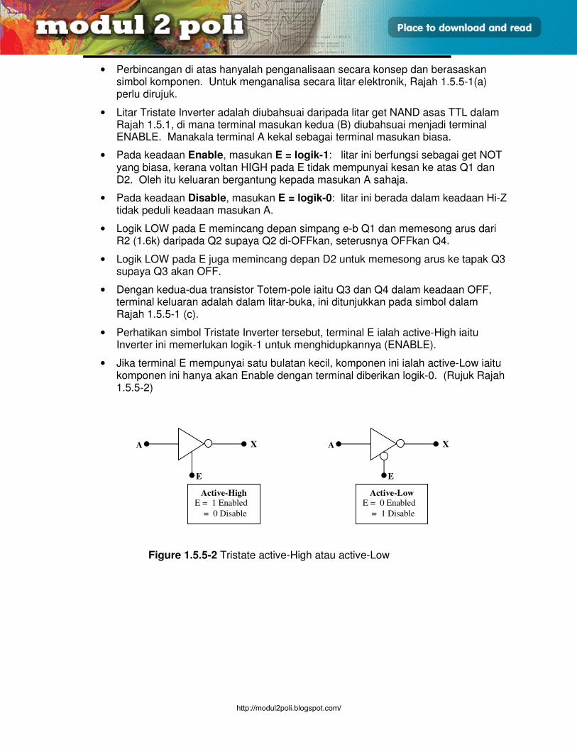
• Perhatikan simbol Tristate Inverter tersebut, terminal E ialah active-High iaitu Inverter ini memerlukan logik-1 untuk menghidupkannya (ENABLE).
• Jika terminal E mempunyai satu bulatan kecil, komponen ini ialah active-Low iaitu komponen ini hanya akan Enable dengan terminal diberikan logik-0. (Rujuk Rajah 1.5.5-2)
Figure 1.5.5-2 Tristate active-High atau active-Low
A X
E
A X
E
Active-High E = 1 Enabled
= 0 Disable
Active-Low E = 0 Enabled
= 1 Disable
http://modul2poli.blogspot.com/
E3165 / UNIT 1 / 24
PEMBINAAN GET LOGIK ASAS
1.6 Current-Sourcing and Current-Singking Action
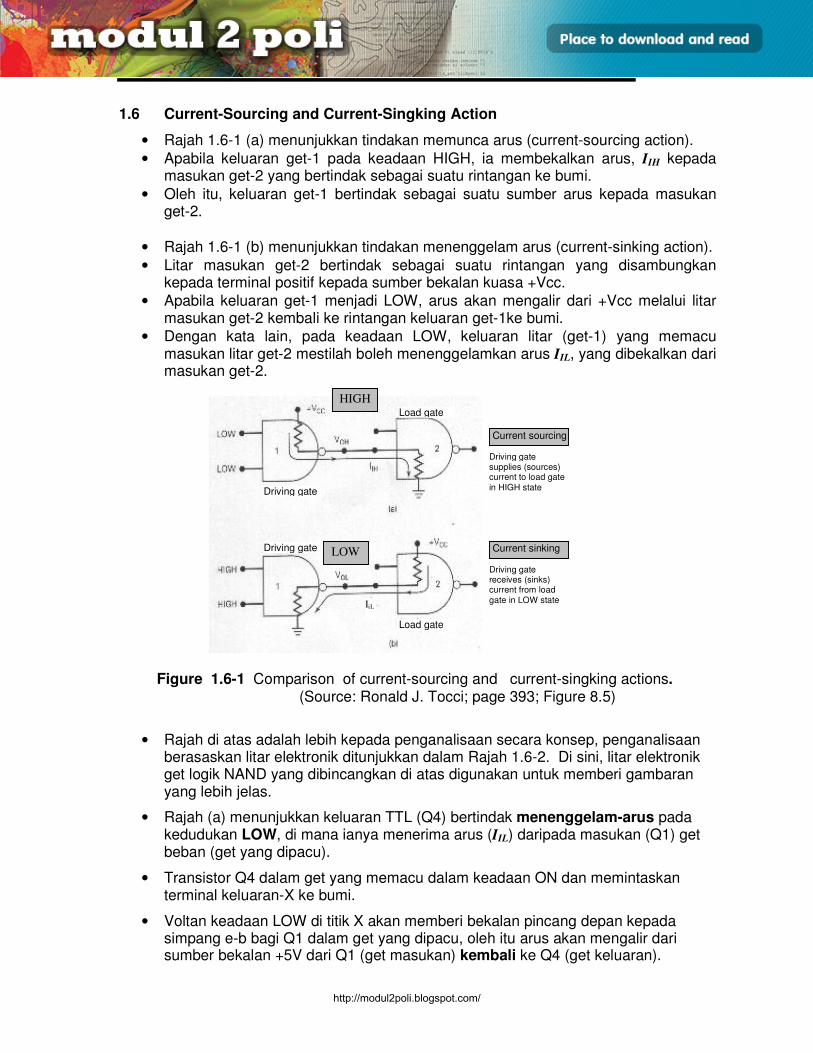
• Rajah 1.6-1 (a) menunjukkan tindakan memunca arus (current-sourcing action).
• Apabila keluaran get-1 pada keadaan HIGH, ia membekalkan arus, IIH kepada masukan get-2 yang bertindak sebagai suatu rintangan ke bumi.
• Oleh itu, keluaran get-1 bertindak sebagai suatu sumber arus kepada masukan get-2.
• Rajah 1.6-1 (b) menunjukkan tindakan menenggelam arus (current-sinking action).
• Litar masukan get-2 bertindak sebagai suatu rintangan yang disambungkan kepada terminal positif kepada sumber bekalan kuasa +Vcc.
• Apabila keluaran get-1 menjadi LOW, arus akan mengalir dari +Vcc melalui litar masukan get-2 kembali ke rintangan keluaran get-1ke bumi.
• Dengan kata lain, pada keadaan LOW, keluaran litar (get-1) yang memacu masukan litar get-2 mestilah boleh menenggelamkan arus IIL, yang dibekalkan dari masukan get-2.
Figure 1.6-1 Comparison of current-sourcing and current-singking actions. (Source: Ronald J. Tocci; page 393; Figure 8.5)
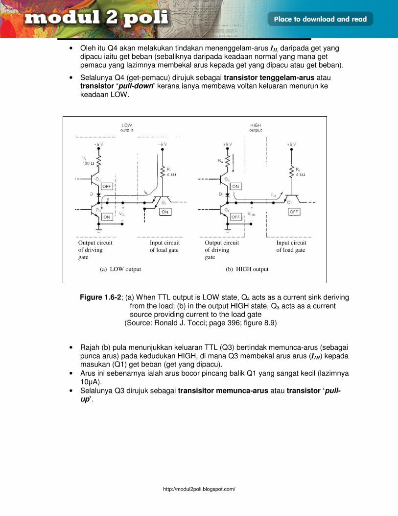
• Rajah di atas adalah lebih kepada penganalisaan secara konsep, penganalisaan berasaskan litar elektronik ditunjukkan dalam Rajah 1.6-2. Di sini, litar elektronik get logik NAND yang dibincangkan di atas digunakan untuk memberi gambaran yang lebih jelas.
• Rajah (a) menunjukkan keluaran TTL (Q4) bertindak menenggelam-arus pada kedudukan LOW, di mana ianya menerima arus (IIL) daripada masukan (Q1) get beban (get yang dipacu).
• Transistor Q4 dalam get yang memacu dalam keadaan ON dan memintaskan terminal keluaran-X ke bumi.
• Voltan keadaan LOW di titik X akan memberi bekalan pincang depan kepada simpang e-b bagi Q1 dalam get yang dipacu, oleh itu arus akan mengalir dari sumber bekalan +5V dari Q1 (get masukan) kembali ke Q4 (get keluaran).
IiL
Driving gate
Driving gate
Load gate
Load gate
Current sourcing
Current sinking
Driving gate supplies (sources) current to load gate in HIGH state
Driving gate receives (sinks) current from load gate in LOW state
HIGH
LOW
http://modul2poli.blogspot.com/
E3165 / UNIT 1 / 25
PEMBINAAN GET LOGIK ASAS
• Oleh itu Q4 akan melakukan tindakan menenggelam-arus IIL daripada get yang dipacu iaitu get beban (sebaliknya daripada keadaan normal yang mana get pemacu yang lazimnya membekal arus kepada get yang dipacu atau get beban).
• Selalunya Q4 (get-pemacu) dirujuk sebagai transistor tenggelam-arus atau transistor ‘pull-down’ kerana ianya membawa voltan keluaran menurun ke keadaan LOW.
Figure 1.6-2; (a) When TTL output is LOW state, Q4 acts as a current sink deriving
from the load; (b) in the output HIGH state, Q3 acts as a current source providing current to the load gate
(Source: Ronald J. Tocci; page 396; figure 8.9)
• Rajah (b) pula menunjukkan keluaran TTL (Q3) bertindak memunca-arus (sebagai punca arus) pada kedudukan HIGH, di mana Q3 membekal arus arus (IIH) kepada masukan (Q1) get beban (get yang dipacu).
• Arus ini sebenarnya ialah arus bocor pincang balik Q1 yang sangat kecil (lazimnya 10µA).
• Selalunya Q3 dirujuk sebagai transisitor memunca-arus atau transistor ‘pull-up’.
Output circuit
of driving
gate
Input circuit
of load gate
(b) HIGH output
Output circuit
of driving
gate
Input circuit
of load gate
(a) LOW output
http://modul2poli.blogspot.com/
E3165 / UNIT 1 / 26
PEMBINAAN GET LOGIK ASAS
1.7 Totem Pole TTL
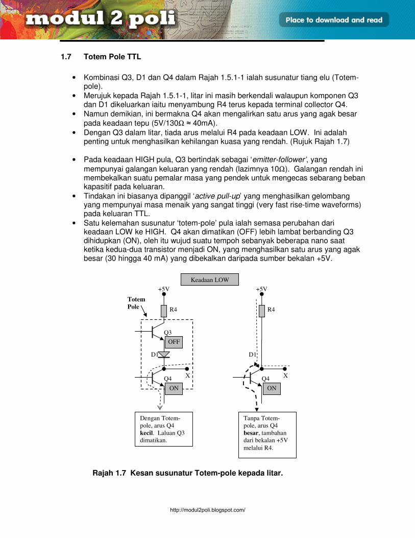
• Kombinasi Q3, D1 dan Q4 dalam Rajah 1.5.1-1 ialah susunatur tiang elu (Totem-pole).
• Merujuk kepada Rajah 1.5.1-1, litar ini masih berkendali walaupun komponen Q3 dan D1 dikeluarkan iaitu menyambung R4 terus kepada terminal collector Q4.
• Namun demikian, ini bermakna Q4 akan mengalirkan satu arus yang agak besar
pada keadaan tepu (5V/130Ω ≈ 40mA).
• Dengan Q3 dalam litar, tiada arus melalui R4 pada keadaan LOW. Ini adalah penting untuk menghasilkan kehilangan kuasa yang rendah. (Rujuk Rajah 1.7)
• Pada keadaan HIGH pula, Q3 bertindak sebagai ‘emitter-follower’, yang
mempunyai galangan keluaran yang rendah (lazimnya 10Ω). Galangan rendah ini membekalkan suatu pemalar masa yang pendek untuk mengecas sebarang beban kapasitif pada keluaran.
• Tindakan ini biasanya dipanggil ‘active pull-up’ yang menghasilkan gelombang yang mempunyai masa menaik yang sangat tinggi (very fast rise-time waveforms) pada keluaran TTL.
• Satu kelemahan susunatur ‘totem-pole’ pula ialah semasa perubahan dari keadaan LOW ke HIGH. Q4 akan dimatikan (OFF) lebih lambat berbanding Q3 dihidupkan (ON), oleh itu wujud suatu tempoh sebanyak beberapa nano saat ketika kedua-dua transistor menjadi ON, yang menghasilkan satu arus yang agak besar (30 hingga 40 mA) yang dibekalkan daripada sumber bekalan +5V.
Rajah 1.7 Kesan susunatur Totem-pole kepada litar.
R4
Q3
D1
Q4
+5V
Totem
Pole R4
D1
Q4
+5V
X X
Keadaan LOW
Dengan Totem-
pole, arus Q4
kecil. Laluan Q3
dimatikan.
Tanpa Totem-
pole, arus Q4
besar, tambahan
dari bekalan +5V
melalui R4.
OFF
ON ON
http://modul2poli.blogspot.com/
E3165 / UNIT 1 / 27
PEMBINAAN GET LOGIK ASAS
1.8 Famili CMOS
• Sebelum kita mengkaji tentang CMOS, adalah lebih baik mengetahui asal usul CMOS iaitu MOS (metal-oxide semiconductor).
• Transisitor berasaskan teknologi MOS ialah ‘field effect transistor’ yang dinamakan MOSFET.
• Terdapat dua jenis MOSFET iaitu ‘depletion’ dan ‘enhancement’.
• Kebanyakan IC digit MOS menggunakan jenis ‘enhancement’.
• Litar-litar digit yang menggunakan MOSFET dibahagikan kepada tiga kategori:
(1) P-MOS yang menggunakan hanya ‘P-channel enhancement MOSFET’ ,
(2) N-MOS menggunakan hanya ‘N-channel enhancement MOSFET’ dan
(3) CMOS (complementary MOS), yang menggunakan kedua-dua peranti P- dan N-channel.
• Secara amnya, CMOS adalah lebih pantas dan penggunaan kuasa yang lebih rendah berbanding famili-famili MOS yang lain, tetapi mempunyai kelemahan dalam aspek kerumitan dalam proses pembuatan IC dan ‘packing density’ (bilangan transistor per cip) yang rendah.
• Famili logik CMOS menggunakan kedua-dua MOSFET ‘p-channel’ dan ‘n-channel’ dalam litar yang sama untuk mengekalkan beberapa kelebihan berbanding famili P-MOS dan N-MOS.
• Oleh itu ada baiknya kita memahami asas kendalian p-channel and n-channel enhancement MOSFET.
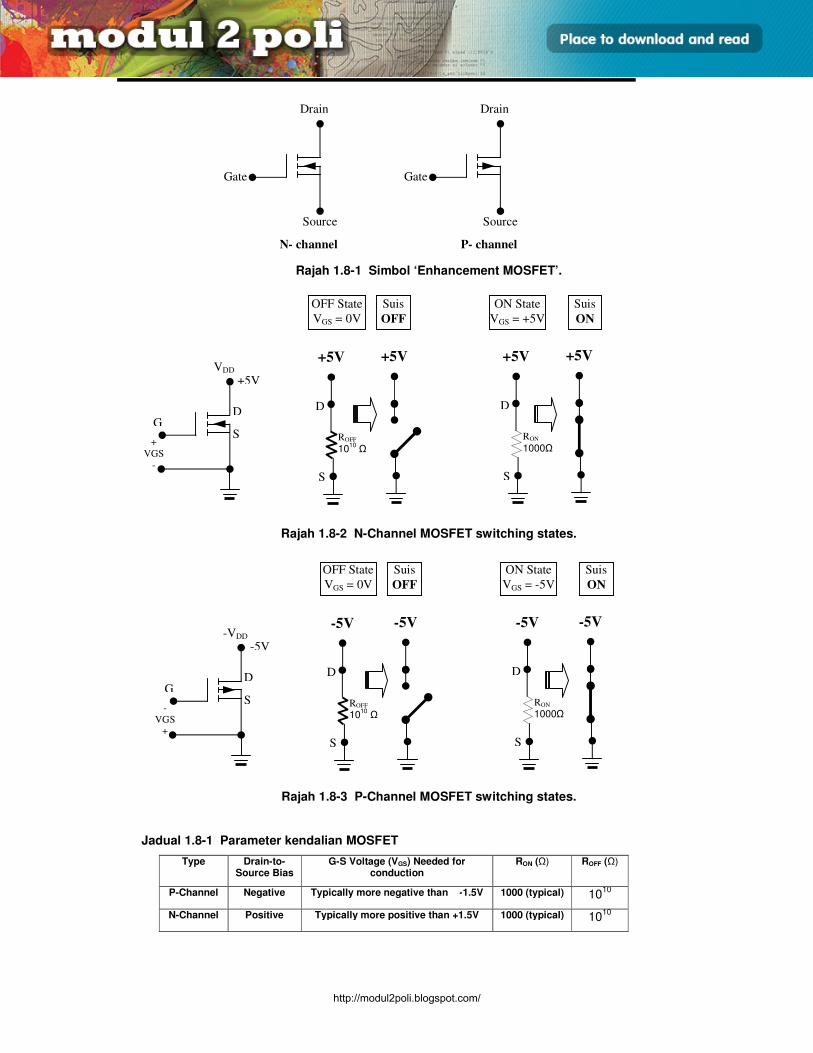
MOSFET p-channel dan n-channel
• Rajah 1.8-1 ialah simbol untuk kedua-dua komponen tersebut. Garis putus-putus antara Drain dan Source menunjukkan dua elektrod ini terbuka pada keadaan biasa. Simbol juga menunjukkan terminal gate dan terminal-terminal yang lain dipisahkan, ini mewakili rintangan yang sangat tinggi (lazimnya 1012 Ω) antara gate dan channel.
• Rajah 1.8-2 menunjukkan operasi penyuisan bagi suatu ‘N-channel MOSFET’.
• Drain sentiasa dipincang positif merujuk kepada Source (+D <> S-). Voltan antara Gate dan Source, VGS ialah voltan masukan, mengawal nilai rintangan antara Drain dan Source (i.e. channel resistance), oleh itu menentukan peranti ini dikendalikan dalam keadaan ON atau OFF.
• Bila VGS = 0V, channel antara Source dan Drain terpisah, dan peranti ini OFF. Lazimnya rintangan channel keadaan OFF ialah 1010 Ω, di mana dalam
INPUT-1E
http://modul2poli.blogspot.com/
E3165 / UNIT 1 / 28
PEMBINAAN GET LOGIK ASAS
kebanyakan keadaan ialah litar terbuka. MOSFET ini akan kekal OFF selagi VGS = 0V atau negatif.
• Bila VGS bernilai positif, (Gate positif merujuk ke Source), apabila VGS mencapai satu nilai voltan VT (Threshold voltage) channel Drain-Source akan mula terbentuk. Lazimnya VT = 1.5V untuk N-MOSFET. Oleh itu, VGS ≥ 1.5V, MOSFET ‘conduct’ (ON). VGS dinaikkan--> channel semakin lebar --> Rchannel semakin mengecil sehingga RON = 1000 Ω.
• Jika dua nilai VGS (0V dan +5V) digunakan untuk mengendalikan komponen ini, maka MOSFET ini berkendali dalam keadaan logik (OFF dan ON).
• MOSFET P-channel berkendali sama seperti MOSFET N-Channel, kecuali bekalan kuasa negatif (-VDD) digunakan, di mana Drain dipincang negatif merujuk Source (-D <> S+). Untuk menghidupkan komponen ini, satu voltan negatif -VGS yang melebihi -VT dikenakan kepada terminal gate. Rajah 1.8-3 menunjukkan keadaan penyuisan tersebut.
• Jadual 1.8-1 membandingkan paramteter untuk kedua-dua N-Channel dan P-channel.
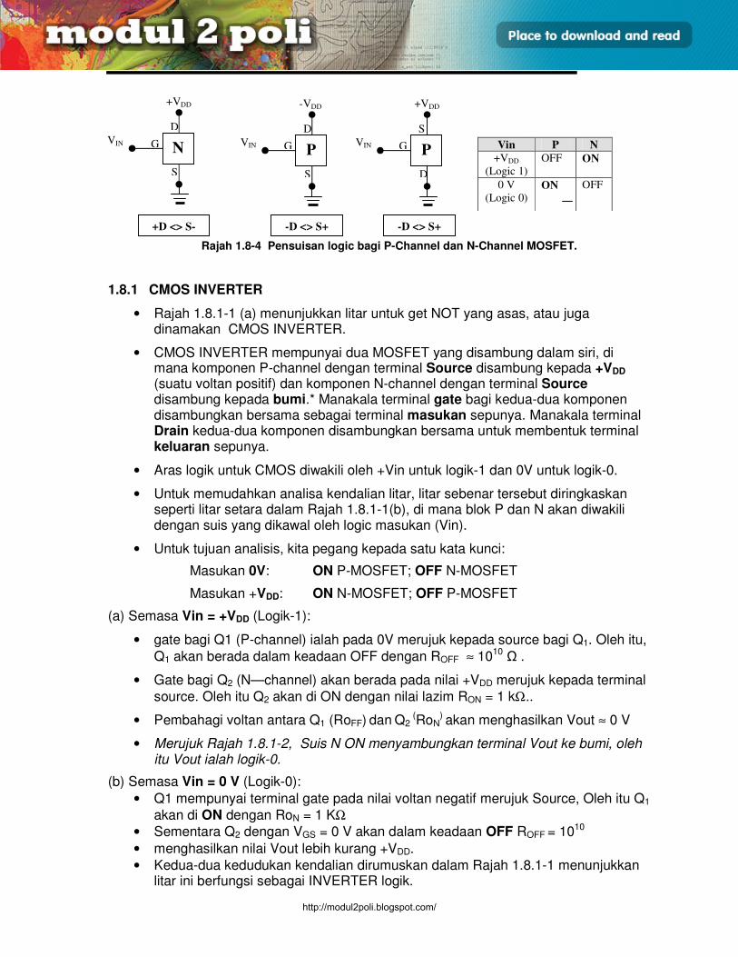
• Untuk memudahkan analisa litar, simbol piawai komponen MOSFET digantikan dengan satu blok yang dilabelkan dengan huruf P dan N untuk mewakili P-MOSFET and N-MOSFET masing-masing.
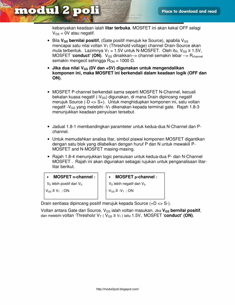
• Rajah 1.8-4 menunjukkan logic pensuisan untuk kedua-dua P- dan N-Channel MOSFET . Rajah ini akan digunakan sebagai rujukan untuk penganalisaan litar-litar berikut.
Drain sentiasa dipincang positif merujuk kepada Source (+D <> S-).
Voltan antara Gate dan Source, VGS ialah voltan masukan, Jika VGS bernilai positif, dan melebihi voltan ‘Threshold’ VT ( VGS ≥ VT ) iaitu 1.5V, MOSFET ‘conduct’ (ON).
• MOSFET n-channel :
VD lebih positif dari VS.
≥ VGS ≥ VT ; ON.
• MOSFET p-channel :
VD lebih negatif dari VS.
≥ -VGS ≥ -VT ; ON
http://modul2poli.blogspot.com/
E3165 / UNIT 1 / 29
PEMBINAAN GET LOGIK ASAS
Rajah 1.8-1 Simbol ‘Enhancement MOSFET’.
Rajah 1.8-2 N-Channel MOSFET switching states.
Rajah 1.8-3 P-Channel MOSFET switching states.
Jadual 1.8-1 Parameter kendalian MOSFET
Type Drain-to-Source Bias
G-S Voltage (VGS) Needed for conduction
RON (Ω) ROFF (Ω)
P-Channel Negative Typically more negative than -1.5V 1000 (typical) 1010
N-Channel Positive Typically more positive than +1.5V 1000 (typical) 1010
Gate
Drain
Source
N- channel
Gate
Drain
Source
P- channel
G
VDD
+
VGS
-
D
S
+5V
+5V +5V
D
S
ROFF
1010
Ω
+5V +5V
D
S
RON
1000Ω
OFF State
VGS = 0V
Suis
OFF
ON State
VGS = +5V
Suis
ON
G
-VDD
-
VGS
+
D
S
-5V
-5V -5V
D
S
ROFF
1010
Ω
-5V -5V
D
S
RON
1000Ω
OFF State
VGS = 0V
Suis
OFF
ON State
VGS = -5V
Suis
ON
http://modul2poli.blogspot.com/
E3165 / UNIT 1 / 30
PEMBINAAN GET LOGIK ASAS
Rajah 1.8-4 Pensuisan logic bagi P-Channel dan N-Channel MOSFET.
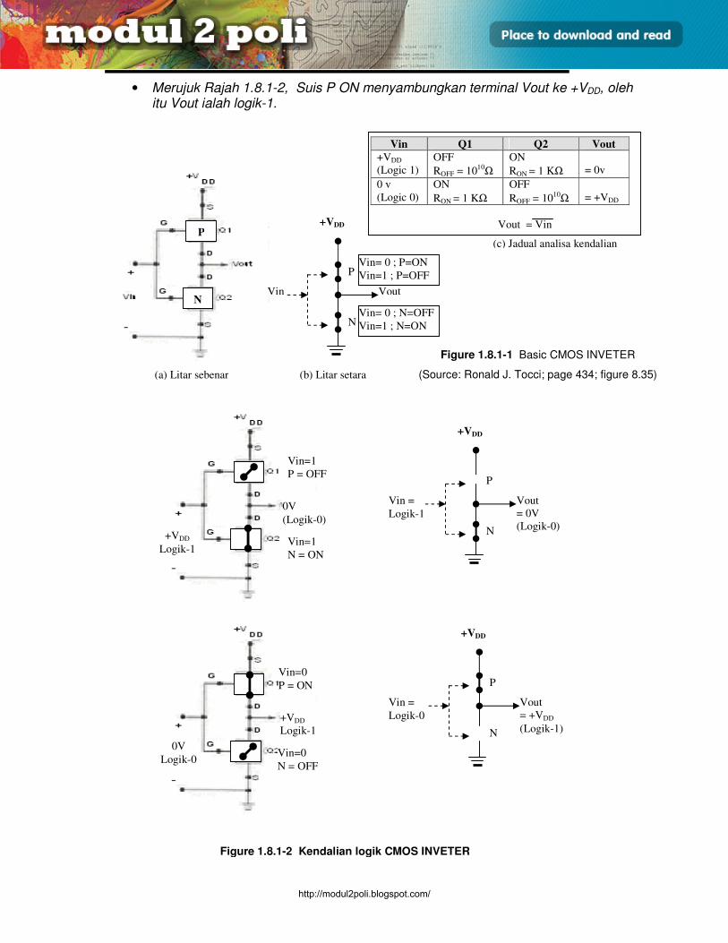
1.8.1 CMOS INVERTER
• Rajah 1.8.1-1 (a) menunjukkan litar untuk get NOT yang asas, atau juga dinamakan CMOS INVERTER.
• CMOS INVERTER mempunyai dua MOSFET yang disambung dalam siri, di mana komponen P-channel dengan terminal Source disambung kepada +VDD (suatu voltan positif) dan komponen N-channel dengan terminal Source disambung kepada bumi.* Manakala terminal gate bagi kedua-dua komponen disambungkan bersama sebagai terminal masukan sepunya. Manakala terminal Drain kedua-dua komponen disambungkan bersama untuk membentuk terminal keluaran sepunya.
• Aras logik untuk CMOS diwakili oleh +Vin untuk logik-1 dan 0V untuk logik-0.
• Untuk memudahkan analisa kendalian litar, litar sebenar tersebut diringkaskan seperti litar setara dalam Rajah 1.8.1-1(b), di mana blok P dan N akan diwakili dengan suis yang dikawal oleh logic masukan (Vin).
• Untuk tujuan analisis, kita pegang kepada satu kata kunci:
Masukan 0V: ON P-MOSFET; OFF N-MOSFET
Masukan +VDD: ON N-MOSFET; OFF P-MOSFET
(a) Semasa Vin = +VDD (Logik-1):
• gate bagi Q1 (P-channel) ialah pada 0V merujuk kepada source bagi Q1. Oleh itu,
Q1 akan berada dalam keadaan OFF dengan ROFF ≈ 1010 Ω .
• Gate bagi Q2 (N—channel) akan berada pada nilai +VDD merujuk kepada terminal
source. Oleh itu Q2 akan di ON dengan nilai lazim RON = 1 kΩ..
• Pembahagi voltan antara Q1 (RoFF) dan Q2 (RoN
) akan menghasilkan Vout ≈ 0 V
• Merujuk Rajah 1.8.1-2, Suis N ON menyambungkan terminal Vout ke bumi, oleh itu Vout ialah logik-0.
(b) Semasa Vin = 0 V (Logik-0):
• Q1 mempunyai terminal gate pada nilai voltan negatif merujuk Source, Oleh itu Q1
akan di ON dengan RoN = 1 KΩ
• Sementara Q2 dengan VGS = 0 V akan dalam keadaan OFF ROFF = 1010
• menghasilkan nilai Vout lebih kurang +VDD.
• Kedua-dua kedudukan kendalian dirumuskan dalam Rajah 1.8.1-1 menunjukkan litar ini berfungsi sebagai INVERTER logik.
Vin P N
+VDD
(Logic 1)
OFF
ON
0 V
(Logic 0) ON
OFF
N
+VDD
D
S
G VIN P
-VDD
D
S
G VIN P
+VDD
S
D
G VIN
+D <> S- -D <> S+ -D <> S+
http://modul2poli.blogspot.com/
E3165 / UNIT 1 / 31
PEMBINAAN GET LOGIK ASAS
• Merujuk Rajah 1.8.1-2, Suis P ON menyambungkan terminal Vout ke +VDD, oleh itu Vout ialah logik-1.
Vin Q1 Q2 Vout
+VDD
(Logic 1)
OFF
ROFF = 1010Ω
ON
RON = 1 KΩ
= 0v
0 v
(Logic 0)
ON
RON = 1 KΩ
OFF
ROFF = 1010Ω
= +VDD
Vout = Vin
P
N
Figure 1.8.1-1 Basic CMOS INVETER
(Source: Ronald J. Tocci; page 434; figure 8.35)
Figure 1.8.1-2 Kendalian logik CMOS INVETER
(a) Litar sebenar (b) Litar setara
(c) Jadual analisa kendalian
+VDD
Vin =
Logik-1
P
Vout
= 0V
(Logik-0) N
+VDD
Vin =
Logik-0
P
Vout
= +VDD
(Logik-1) N
+VDD
Logik-1
0V
(Logik-0)
Vin=1
P = OFF
Vin=1
N = ON
0V
Logik-0
+VDD
Logik-1
Vin=0
P = ON
Vin=0
N = OFF
+VDD
Vin
P
Vout
N
Vin= 0 ; P=ON
Vin=1 ; P=OFF
Vin= 0 ; N=OFF
Vin=1 ; N=ON
http://modul2poli.blogspot.com/
E3165 / UNIT 1 / 32
PEMBINAAN GET LOGIK ASAS
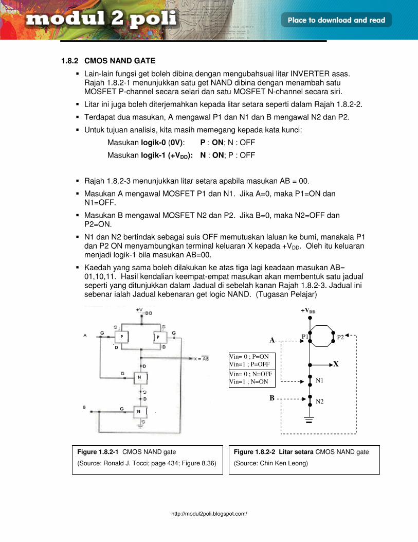
1.8.2 CMOS NAND GATE
Lain-lain fungsi get boleh dibina dengan mengubahsuai litar INVERTER asas. Rajah 1.8.2-1 menunjukkan satu get NAND dibina dengan menambah satu MOSFET P-channel secara selari dan satu MOSFET N-channel secara siri.
Litar ini juga boleh diterjemahkan kepada litar setara seperti dalam Rajah 1.8.2-2.
Terdapat dua masukan, A mengawal P1 dan N1 dan B mengawal N2 dan P2.
Untuk tujuan analisis, kita masih memegang kepada kata kunci:
Masukan logik-0 (0V): P : ON; N : OFF
Masukan logik-1 (+VDD): N : ON; P : OFF
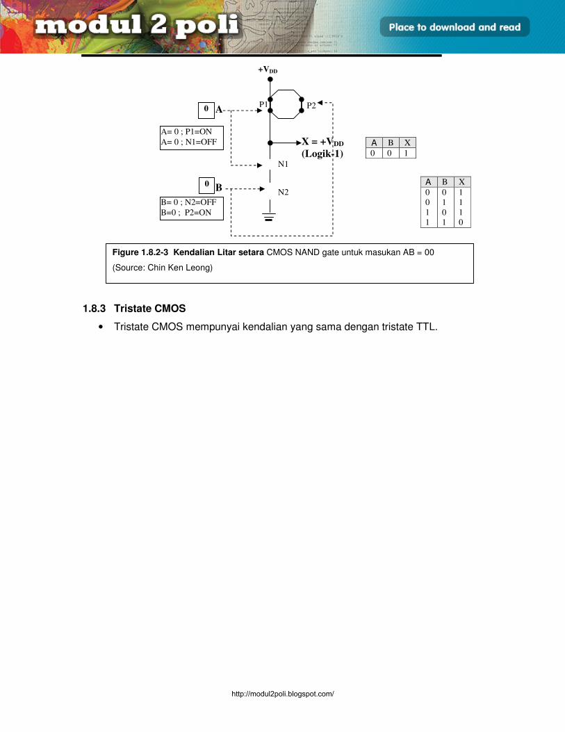
Rajah 1.8.2-3 menunjukkan litar setara apabila masukan AB = 00.
Masukan A mengawal MOSFET P1 dan N1. Jika A=0, maka P1=ON dan N1=OFF.
Masukan B mengawal MOSFET N2 dan P2. Jika B=0, maka N2=OFF dan P2=ON.
N1 dan N2 bertindak sebagai suis OFF memutuskan laluan ke bumi, manakala P1 dan P2 ON menyambungkan terminal keluaran X kepada +VDD. Oleh itu keluaran menjadi logik-1 bila masukan AB=00.
Kaedah yang sama boleh dilakukan ke atas tiga lagi keadaan masukan AB= 01,10,11. Hasil kendalian keempat-empat masukan akan membentuk satu jadual seperti yang ditunjukkan dalam Jadual di sebelah kanan Rajah 1.8.2-3. Jadual ini sebenar ialah Jadual kebenaran get logic NAND. (Tugasan Pelajar)
Figure 1.8.2-1 CMOS NAND gate
(Source: Ronald J. Tocci; page 434; Figure 8.36)
+VDD
A P1
X
N1
Vin= 0 ; P=ON
Vin=1 ; P=OFF
Vin= 0 ; N=OFF
Vin=1 ; N=ON
N2
P2
B
Figure 1.8.2-2 Litar setara CMOS NAND gate
(Source: Chin Ken Leong)
http://modul2poli.blogspot.com/
E3165 / UNIT 1 / 33
PEMBINAAN GET LOGIK ASAS
1.8.3 Tristate CMOS
• Tristate CMOS mempunyai kendalian yang sama dengan tristate TTL.
A B X
0
0
1
1
0
1
0
1
1
1
1
0
+VDD
A P1
X = +VDD
(Logik-1) N1
A= 0 ; P1=ON
A= 0 ; N1=OFF
B= 0 ; N2=OFF
B=0 ; P2=ON
N2
P2
B
0
0
A B X
0 0 1
Figure 1.8.2-3 Kendalian Litar setara CMOS NAND gate untuk masukan AB = 00
(Source: Chin Ken Leong)
http://modul2poli.blogspot.com/
E3165 / UNIT 1 / 34
PEMBINAAN GET LOGIK ASAS
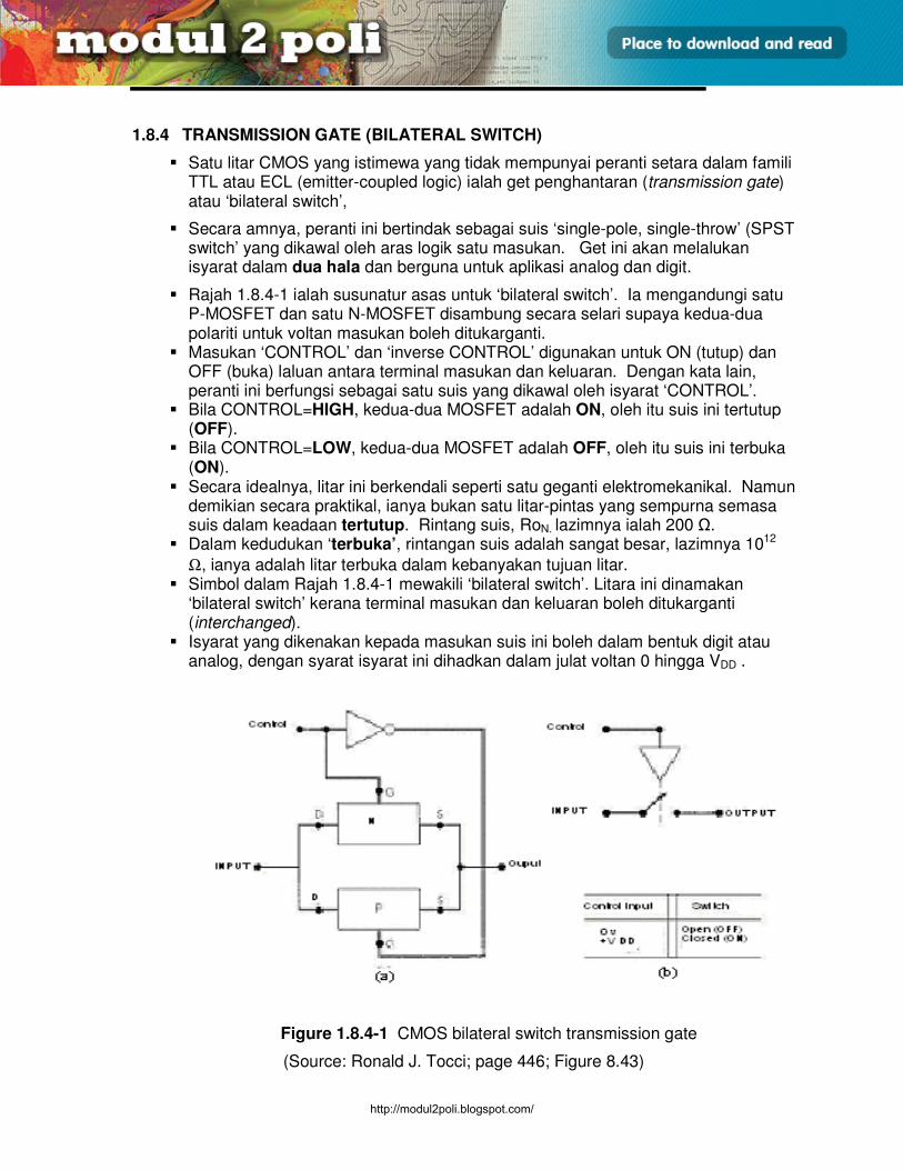
1.8.4 TRANSMISSION GATE (BILATERAL SWITCH)
Satu litar CMOS yang istimewa yang tidak mempunyai peranti setara dalam famili TTL atau ECL (emitter-coupled logic) ialah get penghantaran (transmission gate) atau ‘bilateral switch’,
Secara amnya, peranti ini bertindak sebagai suis ‘single-pole, single-throw’ (SPST switch’ yang dikawal oleh aras logik satu masukan. Get ini akan melalukan isyarat dalam dua hala dan berguna untuk aplikasi analog dan digit.
Rajah 1.8.4-1 ialah susunatur asas untuk ‘bilateral switch’. Ia mengandungi satu P-MOSFET dan satu N-MOSFET disambung secara selari supaya kedua-dua polariti untuk voltan masukan boleh ditukarganti.
Masukan ‘CONTROL’ dan ‘inverse CONTROL’ digunakan untuk ON (tutup) dan OFF (buka) laluan antara terminal masukan dan keluaran. Dengan kata lain, peranti ini berfungsi sebagai satu suis yang dikawal oleh isyarat ‘CONTROL’.
Bila CONTROL=HIGH, kedua-dua MOSFET adalah ON, oleh itu suis ini tertutup (OFF).
Bila CONTROL=LOW, kedua-dua MOSFET adalah OFF, oleh itu suis ini terbuka (ON).
Secara idealnya, litar ini berkendali seperti satu geganti elektromekanikal. Namun demikian secara praktikal, ianya bukan satu litar-pintas yang sempurna semasa suis dalam keadaan tertutup. Rintang suis, RoN. lazimnya ialah 200 Ω.
Dalam kedudukan ‘terbuka’, rintangan suis adalah sangat besar, lazimnya 1012
Ω, ianya adalah litar terbuka dalam kebanyakan tujuan litar. Simbol dalam Rajah 1.8.4-1 mewakili ‘bilateral switch’. Litara ini dinamakan
‘bilateral switch’ kerana terminal masukan dan keluaran boleh ditukarganti (interchanged).
Isyarat yang dikenakan kepada masukan suis ini boleh dalam bentuk digit atau analog, dengan syarat isyarat ini dihadkan dalam julat voltan 0 hingga VDD .
Figure 1.8.4-1 CMOS bilateral switch transmission gate
(Source: Ronald J. Tocci; page 446; Figure 8.43)
http://modul2poli.blogspot.com/
E3165 / UNIT 1 / 35
PEMBINAAN GET LOGIK ASAS
1.8 Perbandingan Siri CMOS dan TTL
Terdapat pelbagai kaedah pembuatan dan corak pembungkusan komponen IC. Namun demikian, kesemua IC ini berkongsi suatu piawaian iaitu ‘universal parameters’. Jadual berikut membandingkan parameter-parameter untuk dua famili IC yang terkenal iaitu TTL dan CMOS.
Parameters TTL CMOS
Noise
Margin
(NM)
Untuk standard TTL, ialah 0.4V seperti dalam Rajah 1.8-1 (a).
Agak baik, dijamin sekurang-kurangnya 30% daripada VDD, 45% adalah secara lazimnya. Seperti dalam Rajah 1.8-1 (a), dengan VDD sebanyak +5V, NM hampiri 1.5V (dengan 45% NM, ianya menghampiri 2.25V). Oleh itu, bila VDD naik, NM turut naik.
Power
Dissipation Keperluan kuasa untuk suatu IC TTL berubah mengikut keperluan arus. Formula kuasa, PAVG = ICC x VCC . Arus masukan dan keluaran untuk dua contoh siri (54XXX/74XXX), untuk kedua-dua aras HIGH dan LOW ( IOH, IOL, IIH and IIL ), seperti ditunjukkan dalam 1.8-1 (b).
Penggunaan kuasa untuk CMOS adalah sangat rendah, dalam nilai 2.5nW (untuk VDD sebanyak +5 v). Bila keluaran menjadi LOW atau HIGH, penggunaan kuasa masih dalam julat nilai 0.5 – 2 mW
Propagation
Delay Propagation delay untuk TTL piawai ditunjukkan dalam Rajah 1.8-1 (c). TPLH lazimnya bernilai 11ns, dengan nilai maksima 22 ns. TPHL lazimnya 7ns, dengan nilai maksima 15 ns.
Propagation delay untuk CMOS adalah lambat berbanding TTL. Kelajuan yang rendah dipengaruhi oleh propagation delays yang agak besar lebih kurang 30-50 ns per gate.
Fan-in Fan-in untuk TTL piawai bergantung hanya kepada bilangan beban unit (unit loads, ul) yang boleh dikendalikan. Lazimnya TTL piawai mempunyai 3.
Fan–in untuk CMOS bergantung kepada bilangan bebana unit (ul) yang boleh dikendalikan. Ianya akan berubah dengan voltan bekalan (VDD).
Fan-out Fan–out untuk siri 54/74 ialah 10. Speed,
Fan-out lazimnya ialah 50 apabila memacu gate CMOS yang lain.
Parameters TTL CMOS
Regulated Power Supply diperlukan Tidak diperlukan
Lengah perambatan rendah tinggi
Kadar kelalian hingar rendah tinggi
Lepasab kuasa tinggi rendah
Penggunaan Teknologi dwikutub pMOS dan nMOS
INPUT-1F
http://modul2poli.blogspot.com/
E3165 / UNIT 1 / 36
PEMBINAAN GET LOGIK ASAS
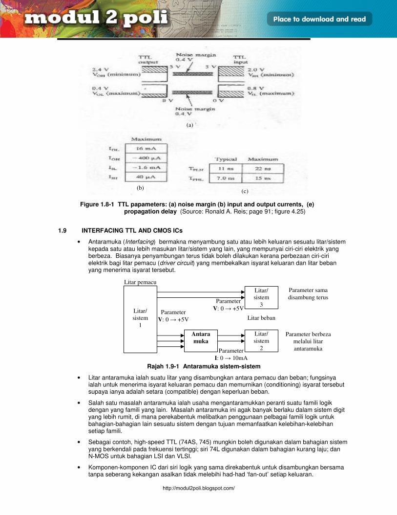
Figure 1.8-1 TTL papameters: (a) noise margin (b) input and output currents, (e) propagation delay (Source: Ronald A. Reis; page 91; figure 4.25)
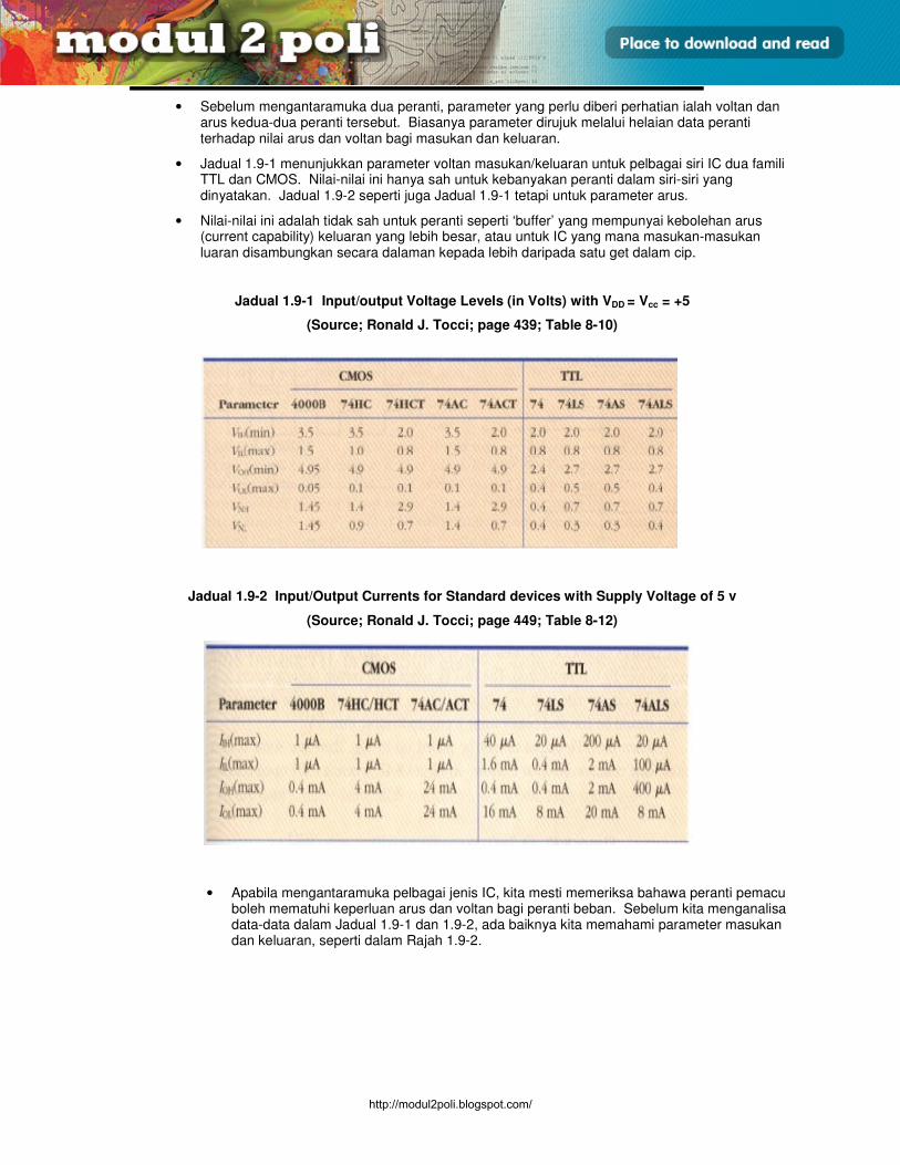
1.9 INTERFACING TTL AND CMOS ICs
• Antaramuka (Interfacing) bermakna menyambung satu atau lebih keluaran sesuatu litar/sistem kepada satu atau lebih masukan litar/sistem yang lain, yang mempunyai ciri-ciri elektrik yang berbeza. Biasanya penyambungan terus tidak boleh dilakukan kerana perbezaan ciri-ciri elektrik bagi litar pemacu (driver circuit) yang membekalkan isyarat keluaran dan litar beban yang menerima isyarat tersebut.
Rajah 1.9-1 Antaramuka sistem-sistem
• Litar antaramuka ialah suatu litar yang disambungkan antara pemacu dan beban; fungsinya ialah untuk menerima isyarat keluaran pemacu dan memurnikan (conditioning) isyarat tersebut supaya ianya adalah setara (compatible) dengan keperluan beban.
• Salah satu masalah antaramuka ialah usaha mengantaramukkan peranti suatu famili logik dengan yang famili yang lain. Masalah antaramuka ini agak banyak berlaku dalam sistem digit yang lebih rumit, di mana perekabentuk melibatkan penggunaan pelbagai famili logik untuk bahagian-bahagian lain sesuatu sistem dengan tujuan memanfaatkan kelebihan-kelebihan setiap famili.
• Sebagai contoh, high-speed TTL (74AS, 745) mungkin boleh digunakan dalam bahagian sistem yang berkendali pada frekuensi tertinggi; siri 74L digunakan dalam bahagian kurang laju; dan N-MOS untuk bahagian LSI dan VLSI.
• Komponen-komponen IC dari siri logik yang sama direkabentuk untuk disambungkan bersama tanpa seberang kekangan asalkan tidak melebihi had-had ‘fan-out’ setiap keluaran.
(a)
(b) (c)
Litar/
sistem
1
Litar/
sistem
2
Antara
muka
Litar pemacu
Litar beban
Parameter
I: 0 → 10mA
Parameter
V: 0 → +5V
Litar/
sistem
3 Parameter
V: 0 → +5V
Parameter berbeza
melalui litar
antaramuka
Parameter sama
disambung terus
http://modul2poli.blogspot.com/
E3165 / UNIT 1 / 37
PEMBINAAN GET LOGIK ASAS
• Sebelum mengantaramuka dua peranti, parameter yang perlu diberi perhatian ialah voltan dan arus kedua-dua peranti tersebut. Biasanya parameter dirujuk melalui helaian data peranti terhadap nilai arus dan voltan bagi masukan dan keluaran.
• Jadual 1.9-1 menunjukkan parameter voltan masukan/keluaran untuk pelbagai siri IC dua famili TTL dan CMOS. Nilai-nilai ini hanya sah untuk kebanyakan peranti dalam siri-siri yang dinyatakan. Jadual 1.9-2 seperti juga Jadual 1.9-1 tetapi untuk parameter arus.
• Nilai-nilai ini adalah tidak sah untuk peranti seperti ‘buffer’ yang mempunyai kebolehan arus (current capability) keluaran yang lebih besar, atau untuk IC yang mana masukan-masukan luaran disambungkan secara dalaman kepada lebih daripada satu get dalam cip.
Jadual 1.9-1 Input/output Voltage Levels (in Volts) with VDD = Vcc = +5
(Source; Ronald J. Tocci; page 439; Table 8-10)
Jadual 1.9-2 Input/Output Currents for Standard devices with Supply Voltage of 5 v
(Source; Ronald J. Tocci; page 449; Table 8-12)
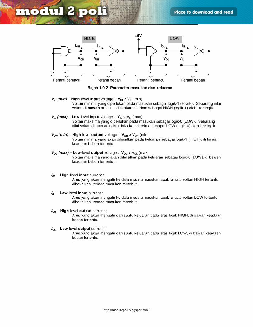
• Apabila mengantaramuka pelbagai jenis IC, kita mesti memeriksa bahawa peranti pemacu boleh mematuhi keperluan arus dan voltan bagi peranti beban. Sebelum kita menganalisa data-data dalam Jadual 1.9-1 dan 1.9-2, ada baiknya kita memahami parameter masukan dan keluaran, seperti dalam Rajah 1.9-2.
http://modul2poli.blogspot.com/
E3165 / UNIT 1 / 38
PEMBINAAN GET LOGIK ASAS
Rajah 1.9-2 Parameter masukan dan keluaran
VIH (min) – High-level input voltage : VIH ≥ VIH (min)
Voltan minima yang diperlukan pada masukan sebagai logik-1 (HIGH). Sebarang nilai voltan di bawah aras ini tidak akan diterima sebagai HIGH (logik-1) oleh litar logik.
VIL (max) – Low-level input voltage : VIL ≤ VIL (max)
Voltan maksima yang diperlukan pada masukan sebagai logik-0 (LOW). Sebarang nilai voltan di atas aras ini tidak akan diterima sebagai LOW (logik-0) oleh litar logik.
VOH (min) – High-level output voltage : VOH ≥ VOH (min)
Voltan minima yang akan dihasilkan pada keluaran sebagai logik-1 (HIGH), di bawah keadaan beban tertentu.
VOL (max) – Low-level output voltage : VOL ≤ VOL (max)
Voltan maksima yang akan dihasilkan pada keluaran sebagai logik-0 (LOW), di bawah keadaan beban tertentu..
IIH – High-level input current : Arus yang akan mengalir ke dalam suatu masukan apabila satu voltan HIGH tertentu dibekalkan kepada masukan tersebut.
IIL – Low-level input current :
Arus yang akan mengalir ke dalam suatu masukan apabila satu voltan LOW tertentu dibekalkan kepada masukan tersebut.
IOH – High-level output current :
Arus yang akan mengalir dari suatu keluaran pada aras logik HIGH, di bawah keadaan beban tertentu..
IOL – Low-level output current :
Arus yang akan mengalir dari suatu keluaran pada aras logik LOW, di bawah keadaan beban tertentu.. .
IOH
HIGH
IIH
+ VOH
¯
+ VIH
¯
IOL
LOW
IIL
+ VOL
¯
+ VIL
¯
+5V
Peranti pemacu Peranti beban Peranti pemacu Peranti beban
http://modul2poli.blogspot.com/
E3165 / UNIT 1 / 39
PEMBINAAN GET LOGIK ASAS
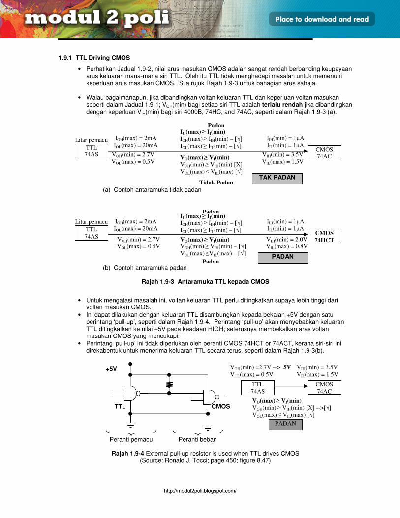
1.9.1 TTL Driving CMOS
• Perhatikan Jadual 1.9-2, nilai arus masukan CMOS adalah sangat rendah berbanding keupayaan arus keluaran mana-mana siri TTL. Oleh itu TTL tidak menghadapi masalah untuk memenuhi keperluan arus masukan CMOS. Sila rujuk Rajah 1.9-3 untuk bahagian arus sahaja.
• Walau bagaimanapun, jika dibandingkan voltan keluaran TTL dan keperluan voltan masukan seperti dalam Jadual 1.9-1; VOH(min) bagi setiap siri TTL adalah terlalu rendah jika dibandingkan dengan keperluan VIH(min) bagi siri 4000B, 74HC, and 74AC, seperti dalam Rajah 1.9-3 (a).
(a) Contoh antaramuka tidak padan
(b) Contoh antaramuka padan
Rajah 1.9-3 Antaramuka TTL kepada CMOS
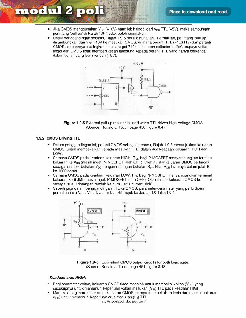
• Untuk mengatasi masalah ini, voltan keluaran TTL perlu ditingkatkan supaya lebih tinggi dari voltan masukan CMOS.
• Ini dapat dilakukan dengan keluaran TTL disambungkan kepada bekalan +5V dengan satu perintang ‘pull-up’, seperti dalam Rajah 1.9-4. Perintang ‘pull-up’ akan menyebabkan keluaran TTL ditingkatkan ke nilai +5V pada keadaan HIGH; seterusnya membekalkan aras voltan masukan CMOS yang mencukupi.
• Perintang ‘pull-up’ ini tidak diperlukan oleh peranti CMOS 74HCT or 74ACT, kerana siri-siri ini direkabentuk untuk menerima keluaran TTL secara terus, seperti dalam Rajah 1.9-3(b).
Rajah 1.9-4 External pull-up resistor is used when TTL drives CMOS (Source: Ronald J. Tocci; page 450; figure 8.47)
TTL
74AS
Litar pemacu
IO(max) ≥ II(min)
IOH(max) ≥ IIH(min) – [√]
IOL(max) ≥ IIL(min) – [√]
IOH(max) = 2mA
IOL(max) = 20mA
CMOS
74AC
IIH(min) = 1µA
IIL(min) = 1µA
Padan
VOH(min) = 2.7V
VOL(max) = 0.5V
VIH(min) = 3.5V
VIL(max) = 1.5V
VO(max) ≥ VI(min)
VOH(min) ≥ VIH(min) [X]
VOL(max) ≤ VIL(max) [√]
Tidak Padan
TAK PADAN
TTL
74AS
Litar pemacu IO(max) ≥ II(min) IOH(max) ≥ IIH(min) – [√]
IOL(max) ≥ IIL(min) – [√]
IOH(max) = 2mA
IOL(max) = 20mA
CMOS
74HCT
IIH(min) = 1µA
IIL(min) = 1µA
Padan
VOH(min) = 2.7V
VOL(max) = 0.5V
VIH(min) = 2.0V
VIL(max) = 0.8V
VO(max) ≥ VI(min)
VOH(min) ≥ VIH(min) – [√]
VOL(max) ≤VIL(max) – [√]
Padan PADAN
TTL
+5V
Peranti pemacu Peranti beban
CMOS
TTL
74AS
CMOS
74AC
VOH(min) =2.7V --> 5V
VOL(max) = 0.5V
VIH(min) = 3.5V
VIL(max) = 1.5V
VO(max) ≥ VI(min)
VOH(min) ≥ VIH(min) [X] -->[√]
VOL(max) ≤ VIL(max) [√]
PADAN
http://modul2poli.blogspot.com/
E3165 / UNIT 1 / 40
PEMBINAAN GET LOGIK ASAS
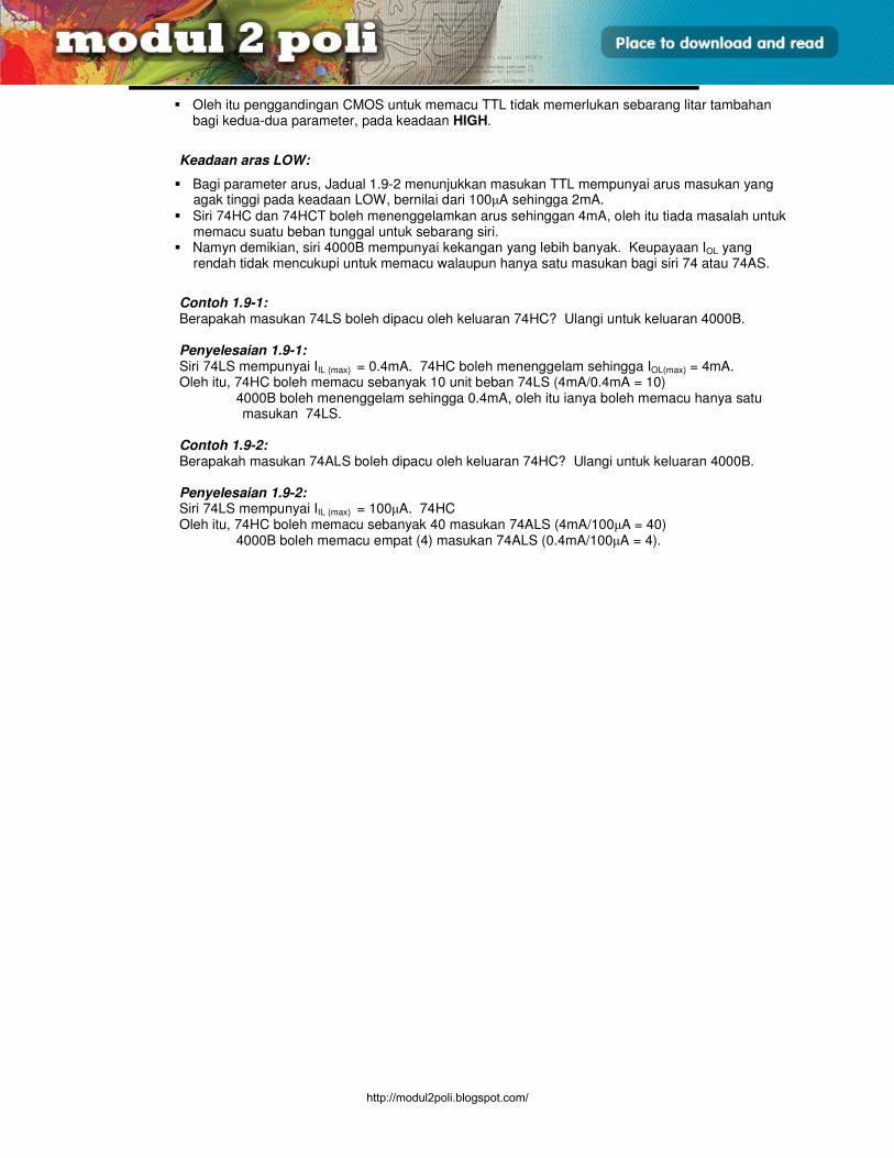
• Jika CMOS menggunakan VDD (+10V) yang lebih tinggi dari VDD TTL (+5V), maka sambungan perintang ‘pull-up’ di Rajah 1.9-4 tidak boleh digunakan.
• Untuk penggandingan sebigini, Rajah 1.9-5 perlu digunakan. Perhatikan, perintang ‘pull-up’ disambungkan dari VDD +10V ke masukan CMOS, di mana peranti TTL (74LS112) dan peranti CMOS sebenarnya diasingkan oleh satu get 7404 iaitu ‘open-collector buffer’, supaya voltan tinggi dari CMOS tidak memberi kesan langsung kepada peranti TTL yang hanya berkendali dalam voltan yang lebih rendah (+5V).
Figure 1.9-5 External pull-up resistor is used when TTL drives High-voltage CMOS
(Source: Ronald J. Tocci; page 450; figure 8.47)
1.9.2 CMOS Driving TTL
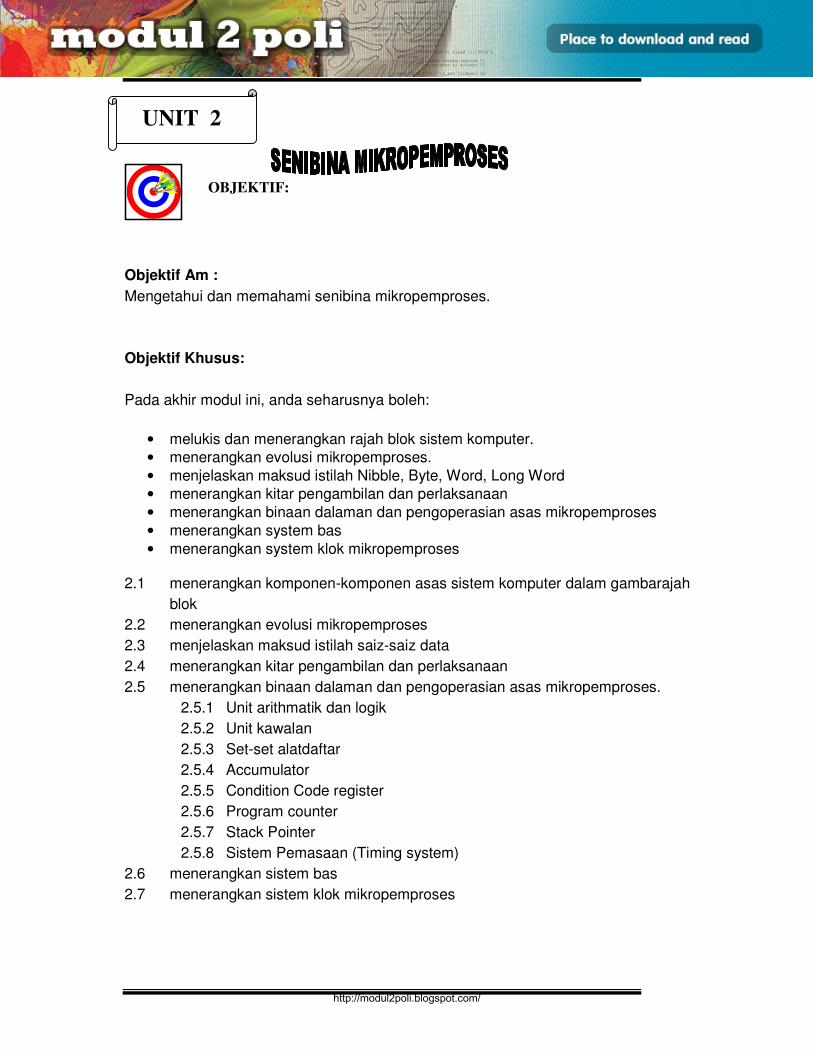
Dalam penggandingan ini, peranti CMOS sebagai pemacu, Rajah 1.9-6 menunjukkan keluaran CMOS (untuk membekalkan kepada masukan TTL) dalam dua keadaan keluaran HIGH dan LOW.
Semasa CMOS pada keadaan keluaran HIGH, RON bagi P-MOSFET menyambungkan terminal keluaran ke VDD (masih ingat, N-MOSFET ialah OFF). Oleh itu litar keluaran CMOS bertindak sebagai sumber bekalan VDD dengan rintangan bekalan Ron. Nilai RON lazimnya dalam julat 100 ke 1000 ohms.
Semasa CMOS pada keadaan keluaran LOW, RON bagi N-MOSFET menyambungkan terminal keluaran ke BUMI (masih ingat, P-MOSFET ialah OFF). Oleh itu litar keluaran CMOS bertindak sebagai suatu rintangan rendah ke bumi, iaitu ‘current sink’.
Seperti juga dalam penggandingan TTL ke CMOS, parameter-parameter yang perlu diberi perhatian iaitu VOH , VOL, IOH , dan IOL. Sila rujuk ke Jadual 1.9-1 dan 1.9-2.
Figure 1.9-6 Equivalent CMOS output circuits for both logic state.
(Source: Ronald J. Tocci; page 451; figure 8.48)
Keadaan aras HIGH:
Bagi parameter voltan, keluaran CMOS tiada masalah untuk membekal voltan (VOH) yang secukupnya untuk memenuhi keperluan voltan masukan (VIH) TTL pada keadaan HIGH.
Manakala bagi parameter arus, keluaran CMOS mampu membekalkan lebih dari mencukupi arus (IOH) untuk memenuhi keperluan arus masukan (IIH) TTL.
http://modul2poli.blogspot.com/
E3165 / UNIT 1 / 41
PEMBINAAN GET LOGIK ASAS
Oleh itu penggandingan CMOS untuk memacu TTL tidak memerlukan sebarang litar tambahan bagi kedua-dua parameter, pada keadaan HIGH.
Keadaan aras LOW:
Bagi parameter arus, Jadual 1.9-2 menunjukkan masukan TTL mempunyai arus masukan yang agak tinggi pada keadaan LOW, bernilai dari 100µA sehingga 2mA.
Siri 74HC dan 74HCT boleh menenggelamkan arus sehinggan 4mA, oleh itu tiada masalah untuk memacu suatu beban tunggal untuk sebarang siri.
Namyn demikian, siri 4000B mempunyai kekangan yang lebih banyak. Keupayaan IOL yang rendah tidak mencukupi untuk memacu walaupun hanya satu masukan bagi siri 74 atau 74AS.
Contoh 1.9-1: Berapakah masukan 74LS boleh dipacu oleh keluaran 74HC? Ulangi untuk keluaran 4000B. Penyelesaian 1.9-1: Siri 74LS mempunyai IIL (max) = 0.4mA. 74HC boleh menenggelam sehingga IOL(max) = 4mA. Oleh itu, 74HC boleh memacu sebanyak 10 unit beban 74LS (4mA/0.4mA = 10)
4000B boleh menenggelam sehingga 0.4mA, oleh itu ianya boleh memacu hanya satu masukan 74LS.
Contoh 1.9-2: Berapakah masukan 74ALS boleh dipacu oleh keluaran 74HC? Ulangi untuk keluaran 4000B. Penyelesaian 1.9-2: Siri 74LS mempunyai IIL (max) = 100µA. 74HC Oleh itu, 74HC boleh memacu sebanyak 40 masukan 74ALS (4mA/100µA = 40)
4000B boleh memacu empat (4) masukan 74ALS (0.4mA/100µA = 4).
http://modul2poli.blogspot.com/
E3165 / UNIT 2 / 1
SENIBINA MIKROPEMPROSES
Objektif Am :
Mengetahui dan memahami senibina mikropemproses.
Objektif Khusus:
Pada akhir modul ini, anda seharusnya boleh:
• melukis dan menerangkan rajah blok sistem komputer.
• menerangkan evolusi mikropemproses.
• menjelaskan maksud istilah Nibble, Byte, Word, Long Word
• menerangkan kitar pengambilan dan perlaksanaan
• menerangkan binaan dalaman dan pengoperasian asas mikropemproses
• menerangkan system bas
• menerangkan system klok mikropemproses 2.1 menerangkan komponen-komponen asas sistem komputer dalam gambarajah
blok
2.2 menerangkan evolusi mikropemproses
2.3 menjelaskan maksud istilah saiz-saiz data
2.4 menerangkan kitar pengambilan dan perlaksanaan
2.5 menerangkan binaan dalaman dan pengoperasian asas mikropemproses.
2.5.1 Unit arithmatik dan logik
2.5.2 Unit kawalan
2.5.3 Set-set alatdaftar
2.5.4 Accumulator
2.5.5 Condition Code register
2.5.6 Program counter
2.5.7 Stack Pointer
2.5.8 Sistem Pemasaan (Timing system)
2.6 menerangkan sistem bas
2.7 menerangkan sistem klok mikropemproses
UNIT 2
OBJEKTIF:
http://modul2poli.blogspot.com/
E3165 / UNIT 2 / 2
SENIBINA MIKROPEMPROSES
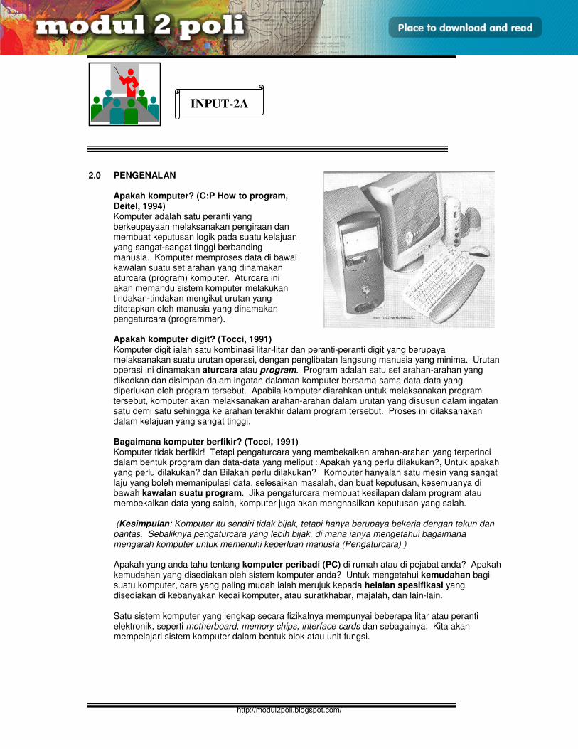
2.0 PENGENALAN Apakah komputer? (C:P How to program, Deitel, 1994) Komputer adalah satu peranti yang berkeupayaan melaksanakan pengiraan dan membuat keputusan logik pada suatu kelajuan yang sangat-sangat tinggi berbanding manusia. Komputer memproses data di bawal kawalan suatu set arahan yang dinamakan aturcara (program) komputer. Aturcara ini akan memandu sistem komputer melakukan tindakan-tindakan mengikut urutan yang ditetapkan oleh manusia yang dinamakan pengaturcara (programmer). Apakah komputer digit? (Tocci, 1991) Komputer digit ialah satu kombinasi litar-litar dan peranti-peranti digit yang berupaya melaksanakan suatu urutan operasi, dengan penglibatan langsung manusia yang minima. Urutan operasi ini dinamakan aturcara atau program. Program adalah satu set arahan-arahan yang dikodkan dan disimpan dalam ingatan dalaman komputer bersama-sama data-data yang diperlukan oleh program tersebut. Apabila komputer diarahkan untuk melaksanakan program tersebut, komputer akan melaksanakan arahan-arahan dalam urutan yang disusun dalam ingatan satu demi satu sehingga ke arahan terakhir dalam program tersebut. Proses ini dilaksanakan dalam kelajuan yang sangat tinggi. Bagaimana komputer berfikir? (Tocci, 1991) Komputer tidak berfikir! Tetapi pengaturcara yang membekalkan arahan-arahan yang terperinci dalam bentuk program dan data-data yang meliputi: Apakah yang perlu dilakukan?, Untuk apakah yang perlu dilakukan? dan Bilakah perlu dilakukan? Komputer hanyalah satu mesin yang sangat laju yang boleh memanipulasi data, selesaikan masalah, dan buat keputusan, kesemuanya di bawah kawalan suatu program. Jika pengaturcara membuat kesilapan dalam program atau membekalkan data yang salah, komputer juga akan menghasilkan keputusan yang salah. (Kesimpulan: Komputer itu sendiri tidak bijak, tetapi hanya berupaya bekerja dengan tekun dan pantas. Sebaliknya pengaturcara yang lebih bijak, di mana ianya mengetahui bagaimana mengarah komputer untuk memenuhi keperluan manusia (Pengaturcara) ) Apakah yang anda tahu tentang komputer peribadi (PC) di rumah atau di pejabat anda? Apakah kemudahan yang disediakan oleh sistem komputer anda? Untuk mengetahui kemudahan bagi suatu komputer, cara yang paling mudah ialah merujuk kepada helaian spesifikasi yang disediakan di kebanyakan kedai komputer, atau suratkhabar, majalah, dan lain-lain. Satu sistem komputer yang lengkap secara fizikalnya mempunyai beberapa litar atau peranti elektronik, seperti motherboard, memory chips, interface cards dan sebagainya. Kita akan mempelajari sistem komputer dalam bentuk blok atau unit fungsi.
INPUT-2A
http://modul2poli.blogspot.com/
E3165 / UNIT 2 / 3
SENIBINA MIKROPEMPROSES
2.1 GAMBARAJAH BLOK SISTEM KOMPUTER ASAS
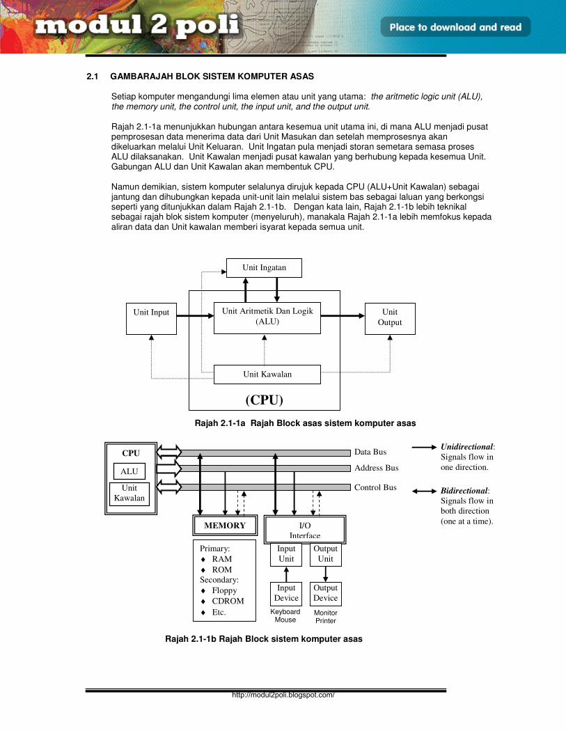
Setiap komputer mengandungi lima elemen atau unit yang utama: the aritmetic logic unit (ALU), the memory unit, the control unit, the input unit, and the output unit. Rajah 2.1-1a menunjukkan hubungan antara kesemua unit utama ini, di mana ALU menjadi pusat pemprosesan data menerima data dari Unit Masukan dan setelah memprosesnya akan dikeluarkan melalui Unit Keluaran. Unit Ingatan pula menjadi storan semetara semasa proses ALU dilaksanakan. Unit Kawalan menjadi pusat kawalan yang berhubung kepada kesemua Unit. Gabungan ALU dan Unit Kawalan akan membentuk CPU. Namun demikian, sistem komputer selalunya dirujuk kepada CPU (ALU+Unit Kawalan) sebagai jantung dan dihubungkan kepada unit-unit lain melalui sistem bas sebagai laluan yang berkongsi seperti yang ditunjukkan dalam Rajah 2.1-1b. Dengan kata lain, Rajah 2.1-1b lebih teknikal sebagai rajah blok sistem komputer (menyeluruh), manakala Rajah 2.1-1a lebih memfokus kepada aliran data dan Unit kawalan memberi isyarat kepada semua unit.
Rajah 2.1-1a Rajah Block asas sistem komputer asas
MEMORY
Primary:
♦ RAM
♦ ROM
Secondary:
♦ Floppy
♦ CDROM
♦ Etc.
I/O
Interface
Input
Unit
Data Bus
Address Bus
Control Bus
Unidirectional:
Signals flow in
one direction.
Bidirectional:
Signals flow in
both direction
(one at a time).
Rajah 2.1-1b Rajah Block sistem komputer asas
CPU
ALU
Unit
Kawalan
Output
Unit
Input
Device
Output
Device
Keyboard Mouse
Monitor Printer
Unit Aritmetik Dan Logik
(ALU)
Unit Kawalan
Unit Ingatan
Unit Input Unit
Output
(CPU)
http://modul2poli.blogspot.com/
E3165 / UNIT 2 / 4
SENIBINA MIKROPEMPROSES
FUNGSI BAGI SETIAP KOMPONEN/UNIT SISTEM KOMPUTER ASAS :
Unit Aritmetik dan Logik (ALU):
Unit yang melaksanakan operasi komputer. Ia menerima suruhan-suruhan dan data untuk melaksanakan proses arithmetik dan logik.
Proses arithmetik ialah seperti campur, tolak, darab dan bahagi (+, -, x, /). manakala proses logik ialah menentukan samada sama atau tidak sama melalui operasi
logik AND, OR, NOT, EXOR dan sebagainya. Dalam sistem industri perkilangan, Unit ALU seperti Bahagian pembuatan
(manufacuring). Unit Kawalan:
Unit ini mengarah operasi kesemua unit dengan menyediakan isyarat pemasaan dan kawalan (timing and control signal).
Unit ALU hanya melaksanakan sesuatu tugas hanya dengan arahan daripada unit kawalan dalam bentuk: Apakah? Dari manakah? Ke manakah? Bilakah? Berapa lamakah?
Unit ini mengandungi litar logik dan pemasaan yang menjana isyarat yang sesuai untuk memantau perlaksanakan setiap arahan dalam aturcara.
Unit ini melaksanakan dua kitar utama iaitu kitar capai (fetch) dan kitar laksana (execute), dan dua proses ini sahaja sebenarnya akan diulang-ulang sepanjang perlaksaan sistem komputer.
Dalam sistem industri perkilangan, Unit keluaran seperti Bahagian pentadbiran (administartive).
Central Processing Unit (CPU):
Gabungan kedua-dua unit ALU dan Kawalan akan membentuk CPU, dan menjadi elemen utama sistem komputer seperti jantung untuk manusia.
CPU selalu dibina dalam satu chip tunggal untuk mengasingkan lain-lain unit dalam satu sistem komputer. Chip CPU ini selalunya dipanggil mikroprocessor atau microprocessor chip.
Unit masukan:
Unit ini memperolehi/menerima maklumat (data dan aturcara komputer) dari pelbagai peranti masukan seperti keyboard, scanner, joystick dan lain-lain.
Unit ini juga menyediakan maklumat ini untuk dicapai oleh unit-unit yang lain contohnya ALU, ingatan.
Dalam sistem industri perkilangan, unit masukan seperi Bahagian penerimaan.
Unit Keluaran: Unit ini memindah data dan maklumat yang telah diproses oleh komputer (ALU) atau
maklumat dalam ingatan ke persekitaran luar komputer melalui peranti-peranti keluaran, seperti monitor, pencetak dll.
Dalam sistem industri perkilangan, Unit keluaran seperti Bahagian penghantaran. Unit I/O:
Unit ini sebenarnya ialah gabungan kedua-dua unit masukan dan keluaran (Input/Output). I/O interface menjadi perantara (antaramuka) antara Unit Masukan/ Unit Keluaran dengan
system computer. Bentuk isyarat/maklumat di luar dan dalam computer mungkin berbeza oleh itu I/O
interface diperlukan mengubah bentuk isyarat supaya setara dengan peringkat yang digandingkan.
Unit ingatan:
Unit ini menyimpan maklumat yang telah dimasukkan melalui unit masukan supaya maklumat ini sedia dicapai terus untuk diproses apabila diperlukan.
Unit ini juga menyimpan maklumat yang telah diproses oleh komputer (ALU) sehingga maklumat ini bersedia diterima oleh unit keluaran.
http://modul2poli.blogspot.com/
E3165 / UNIT 2 / 5
SENIBINA MIKROPEMPROSES
Unit ini mengandungi RAM dan ROM yang selalu dipanggil ingatan utama/primer. Dalam sistem industri perkilangan, Unit ingatan seperti Bahagian gudang/ warehouse. Selain ingatan utama (dalaman) sistem komputer biasanya disokong oleh ingatan
tambahan yang biasanya dikenali sebagai ingatan sekunder (luaran) seperti floppy disk, CD-ROM dan lain-lain.
Sistem Bas (Bus system)
♦ Dawai biasanya digunakan untuk memindahkan suatu isyarat dari satu titik ke titik yang lain. Satu kumpulan dawai-dawai dinamakan bas.
♦ Dalam sistem mikrokomputer, terdapat 3 bas iaitu data (data), alamat (address), and kawalan (control) untuk menghubungkan mikropemproses (CPU) kepada setiap peranti dalam sistem mikrokomputer seperti ingatan dan peranti I/O.
♦ Bas-bas ini akan membawa (hantar atau terima) kesemua maklumat dan isyarat yang terlibat dalam operasi sistem dari satu peranti ke peranti yang lain.
Data bus:
♦ Membawa isyarat yang mewakili data dari satu peranti ke pertanti yang lain: Dari CPU ke ingatan, dan sebaliknya. Dari CPU ke Unit Keluaran. Dari Ingatan ke Unit Keluaran Dari Unit Masukan ke CPU/Ingatan.
♦ Bas dua hala (Bidirectional bus), kerana data boleh mengalir ke atau dari CPU.
♦ Saiz bas data ditentukan oleh bilangan talian (bit) data yang juga dipanggil saiz data.
♦ Saiz data: Saiz sel individu dalam ingatan Bilangan bit yang boleh dikendalikan oleh CPU pada satu-satu ketika.
♦ Mikropemproses MC68000 mempunyai bas data 32 bit, oleh itu: Saiz Data, n = 32 bits, Talian Data dilabel, Dn : D0, D1, ….. D30, D31
♦ Dengan kata lain, CPU boleh mengendalikan, atau bas data boleh memindahkan, data 8 bit secara selari/serentak, seterusnya menjadi penentu kelajuan pemindahan data.
♦ Bas (Bit) data yang sama boleh diset menjadi samada masukan atau keluaran bergantung kepada proses CPU melaksanakan operasi samada membaca (read) atau menulis (write) masing-masing.
CPU
R/W
Control signal is
Logic-1 =
R: READ
Input (from
Memory or
I/O devices)
CPU
R/W
Control signal is
Logic-0 = W:
WRITE
Output (to Memory
or I/O
devices)
Data bus Data bus
CPU
Memory I/O
Devices
CPU to other elements DATA BUS
From other elements
to CPU
http://modul2poli.blogspot.com/
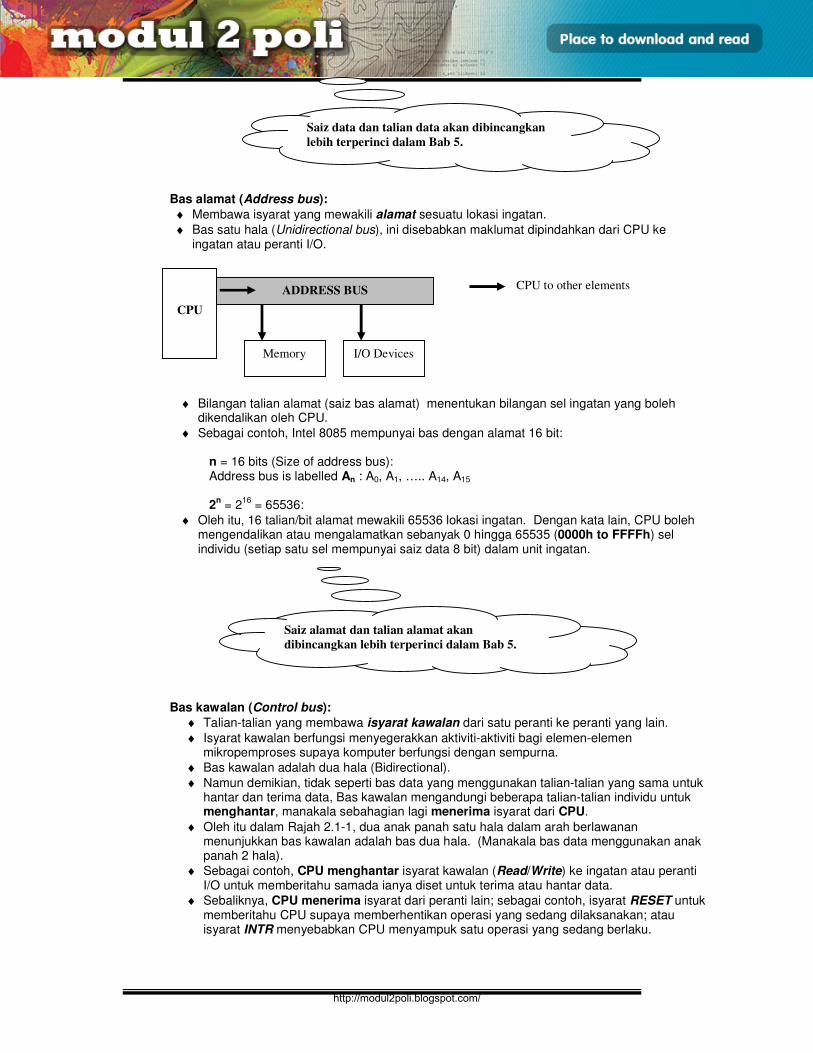
E3165 / UNIT 2 / 6
SENIBINA MIKROPEMPROSES
Bas alamat (Address bus):
♦ Membawa isyarat yang mewakili alamat sesuatu lokasi ingatan.
♦ Bas satu hala (Unidirectional bus), ini disebabkan maklumat dipindahkan dari CPU ke ingatan atau peranti I/O.
♦ Bilangan talian alamat (saiz bas alamat) menentukan bilangan sel ingatan yang boleh dikendalikan oleh CPU.
♦ Sebagai contoh, Intel 8085 mempunyai bas dengan alamat 16 bit:
n = 16 bits (Size of address bus): Address bus is labelled An : A0, A1, ….. A14, A15
2
n = 2
16 = 65536:
♦ Oleh itu, 16 talian/bit alamat mewakili 65536 lokasi ingatan. Dengan kata lain, CPU boleh mengendalikan atau mengalamatkan sebanyak 0 hingga 65535 (0000h to FFFFh) sel individu (setiap satu sel mempunyai saiz data 8 bit) dalam unit ingatan.
Bas kawalan (Control bus):
♦ Talian-talian yang membawa isyarat kawalan dari satu peranti ke peranti yang lain.
♦ Isyarat kawalan berfungsi menyegerakkan aktiviti-aktiviti bagi elemen-elemen mikropemproses supaya komputer berfungsi dengan sempurna.
♦ Bas kawalan adalah dua hala (Bidirectional).
♦ Namun demikian, tidak seperti bas data yang menggunakan talian-talian yang sama untuk hantar dan terima data, Bas kawalan mengandungi beberapa talian-talian individu untuk menghantar, manakala sebahagian lagi menerima isyarat dari CPU.
♦ Oleh itu dalam Rajah 2.1-1, dua anak panah satu hala dalam arah berlawanan menunjukkan bas kawalan adalah bas dua hala. (Manakala bas data menggunakan anak panah 2 hala).
♦ Sebagai contoh, CPU menghantar isyarat kawalan (Read/Write) ke ingatan atau peranti I/O untuk memberitahu samada ianya diset untuk terima atau hantar data.
♦ Sebaliknya, CPU menerima isyarat dari peranti lain; sebagai contoh, isyarat RESET untuk memberitahu CPU supaya memberhentikan operasi yang sedang dilaksanakan; atau isyarat INTR menyebabkan CPU menyampuk satu operasi yang sedang berlaku.
CPU
Memory I/O Devices
CPU to other elements ADDRESS BUS
Saiz data dan talian data akan dibincangkan
lebih terperinci dalam Bab 5.
Saiz alamat dan talian alamat akan
dibincangkan lebih terperinci dalam Bab 5.
http://modul2poli.blogspot.com/
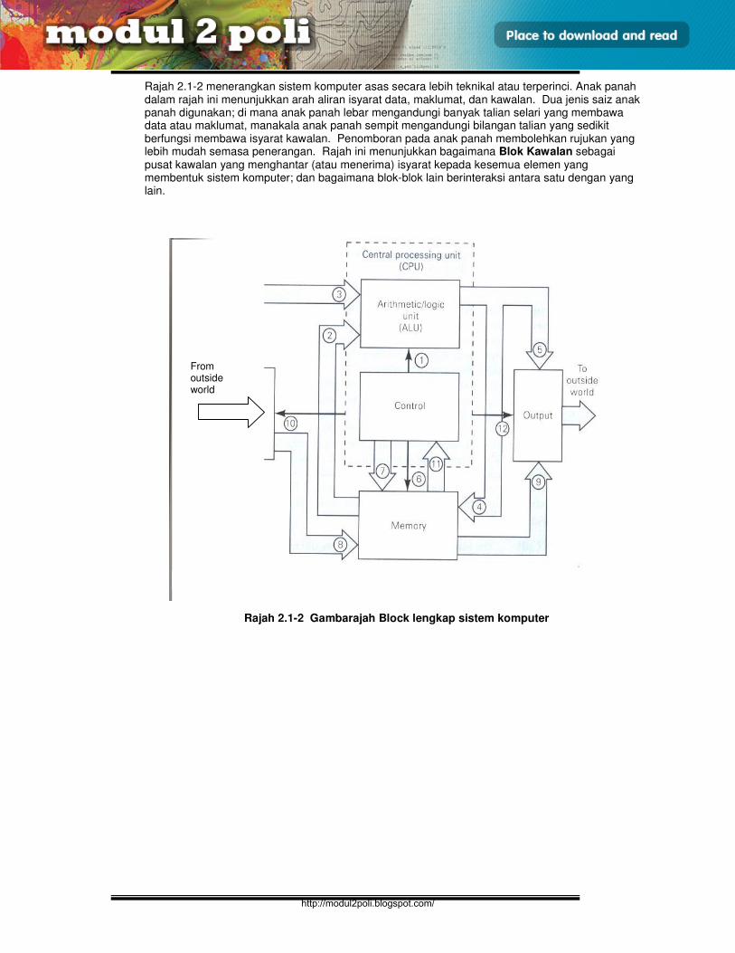
E3165 / UNIT 2 / 7
SENIBINA MIKROPEMPROSES
Rajah 2.1-2 menerangkan sistem komputer asas secara lebih teknikal atau terperinci. Anak panah dalam rajah ini menunjukkan arah aliran isyarat data, maklumat, dan kawalan. Dua jenis saiz anak panah digunakan; di mana anak panah lebar mengandungi banyak talian selari yang membawa data atau maklumat, manakala anak panah sempit mengandungi bilangan talian yang sedikit berfungsi membawa isyarat kawalan. Penomboran pada anak panah membolehkan rujukan yang lebih mudah semasa penerangan. Rajah ini menunjukkan bagaimana Blok Kawalan sebagai pusat kawalan yang menghantar (atau menerima) isyarat kepada kesemua elemen yang membentuk sistem komputer; dan bagaimana blok-blok lain berinteraksi antara satu dengan yang lain.
Rajah 2.1-2 Gambarajah Block lengkap sistem komputer
From outside world
http://modul2poli.blogspot.com/
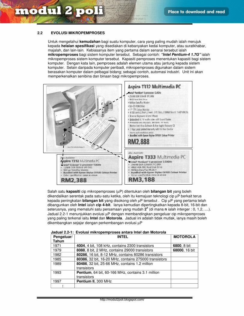
E3165 / UNIT 2 / 8
SENIBINA MIKROPEMPROSES
2.2 EVOLUSI MIKROPEMPROSES
Untuk mengetahui kemudahan bagi suatu komputer, cara yang paling mudah ialah merujuk kepada helaian spesifikasi yang disediakan di kebanyakan kedai komputer, atau suratkhabar, majalah, dan lain-lain. Kebiasanya item yang pertama dalam senarai tersebut ialah mikropemproses bagi sistem komputer tersebut. Sebagai contoh: “Intel Pentium-4 1.7G” ialah mikropemproses sistem komputer tersebut. Kapasiti pemproses menentukan kapasiti bagi sistem komputer. Dengan kata lain, pemproses adalah elemen utama atau jantung kepada sistem komputer. Selain daripada komputer peribadi, mikropemproses digunakan dalam sistem berasakan komputer dalam pelbagai bidang; sebagai contoh, automasi industri. Unit ini akan memperkenalkan senibina dan binaan bagi mikropemproses.
Salah satu kapasiti cip mikropemproses (µP) ditentukan oleh bilangan bit yang boleh
dikendalikan serentak pada satu-satu ketika, oleh itu kemajuan teknologi cip µP berkait terus
kepada peningkatan bilangan bit yang disokong oleh µP tersebut . Cip µP yang pertama telah dibangunkan oleh Intel ialah cip 4-bit. Ianya kemudian dipertingkatkan kepada 8-bit, 16-bit dan seterusnya, yang mematuhi satu persamaan yang mudah 2
n (di mana n ialah interger : 0, 1,2, ....).
Jadual 2.2-1 menunjukkan evolusi µP dengan membandingkan pengeluar cip mikropemproses yang paling terkenal iaitu Intel dan Motorola. Jadual ini adalah tidak mutlak, ianya masih boleh
dikembangkan sejajar dengan perkembangan evolusi µP
Jadual 2.2-1: Evolusi mikropemproses antara Intel dan Motorola
Pengeluar/ Tahun
INTEL MOTOROLA
1971 4004, 4 bit, 108 kHz, contains 2300 transistors 6800, 8 bit
1979 8088, 8 bit, 2 MHz, contains 29000 transistors 68000, 16 bit
1982 80286, 16 bit, 8-12 MHz, contains 80286 transistors
1985 80386, 32 bit, 16-20 MHz, contains 275000 transistors
1989 80486, 32 bit, 25-66 MHz, contains 1.2 million transistors
1993 Pentium, 64 bit, 60-166 MHz, contains 3.1 million transistors
1997 Pentium II, 300 MHz
:
http://modul2poli.blogspot.com/
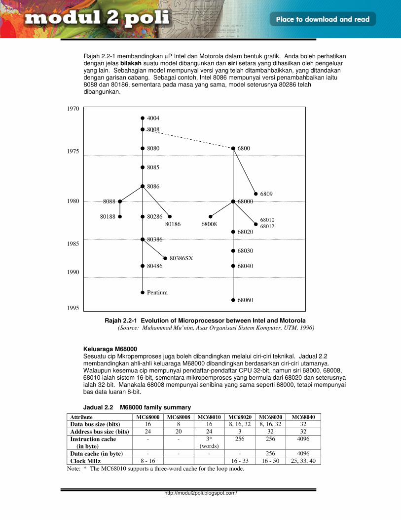
E3165 / UNIT 2 / 9
SENIBINA MIKROPEMPROSES
Rajah 2.2-1 membandingkan µP Intel dan Motorola dalam bentuk grafik. Anda boleh perhatikan dengan jelas bilakah suatu model dibangunkan dan siri setara yang dihasilkan oleh pengeluar yang lain. Sebahagian model mempunyai versi yang telah ditambahbaikkan, yang ditandakan dengan garisan cabang. Sebagai contoh, Intel 8086 mempunyai versi penambahbaikan iaitu 8088 dan 80186, sementara pada masa yang sama, model seterusnya 80286 telah dibangunkan.
Rajah 2.2-1 Evolution of Microprocessor between Intel and Motorola (Source: Muhammad Mu’nim, Asas Organisasi Sistem Komputer, UTM, 1996)
Keluaraga M68000 Sesuatu cip Mkropemproses juga boleh dibandingkan melalui ciri-ciri teknikal. Jadual 2.2 membandingkan ahli-ahli keluaraga M68000 dibandingkan berdasarkan ciri-ciri utamanya. Walaupun kesemua cip mempunyai pendaftar-pendaftar CPU 32-bit, namun siri 68000, 68008, 68010 ialah sistem 16-bit, sementara mikropemproses yang bermula dari 68020 dan seterusnya ialah 32-bit. Manakala 68008 mempunyai senibina yang sama seperti 68000, tetapi mempunyai bas data luaran 8-bit.
Jadual 2.2 M68000 family summary
4004
8008
8080
8085
8086
80286
80386
80486
Pentium
80186
8088
80188
80386SX
6800
68000
68020
6809
68010
68012 68008
68030
68040
68060
1970
1975
1980
1985
1990
1995
Attribute MC68000 MC68008 MC68010 MC68020 MC68030 MC68040
Data bus size (bits) 16 8 16 8, 16, 32 8, 16, 32 32
Address bus size (bits) 24 20 24 3 32 32
Instruction cache
(in byte)
- - 3*
(words)
256 256 4096
Data cache (in byte) - - - - 256 4096
Clock MHz 8 - 16 16 - 33 16 - 50 25, 33, 40
Note: * The MC68010 supports a three-word cache for the loop mode.
http://modul2poli.blogspot.com/
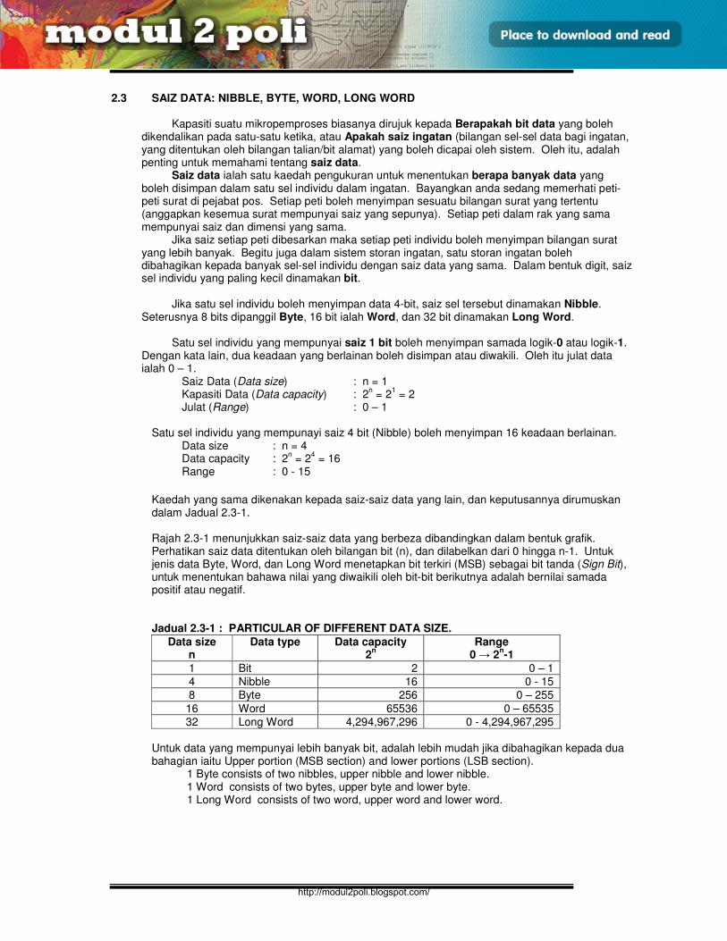
E3165 / UNIT 2 / 10
SENIBINA MIKROPEMPROSES
2.3 SAIZ DATA: NIBBLE, BYTE, WORD, LONG WORD
Kapasiti suatu mikropemproses biasanya dirujuk kepada Berapakah bit data yang boleh
dikendalikan pada satu-satu ketika, atau Apakah saiz ingatan (bilangan sel-sel data bagi ingatan, yang ditentukan oleh bilangan talian/bit alamat) yang boleh dicapai oleh sistem. Oleh itu, adalah penting untuk memahami tentang saiz data.
Saiz data ialah satu kaedah pengukuran untuk menentukan berapa banyak data yang boleh disimpan dalam satu sel individu dalam ingatan. Bayangkan anda sedang memerhati peti-peti surat di pejabat pos. Setiap peti boleh menyimpan sesuatu bilangan surat yang tertentu (anggapkan kesemua surat mempunyai saiz yang sepunya). Setiap peti dalam rak yang sama mempunyai saiz dan dimensi yang sama.
Jika saiz setiap peti dibesarkan maka setiap peti individu boleh menyimpan bilangan surat yang lebih banyak. Begitu juga dalam sistem storan ingatan, satu storan ingatan boleh dibahagikan kepada banyak sel-sel individu dengan saiz data yang sama. Dalam bentuk digit, saiz sel individu yang paling kecil dinamakan bit.
Jika satu sel individu boleh menyimpan data 4-bit, saiz sel tersebut dinamakan Nibble.
Seterusnya 8 bits dipanggil Byte, 16 bit ialah Word, dan 32 bit dinamakan Long Word. Satu sel individu yang mempunyai saiz 1 bit boleh menyimpan samada logik-0 atau logik-1.
Dengan kata lain, dua keadaan yang berlainan boleh disimpan atau diwakili. Oleh itu julat data ialah 0 – 1.
Saiz Data (Data size) : n = 1 Kapasiti Data (Data capacity) : 2
n = 2
1 = 2
Julat (Range) : 0 – 1 Satu sel individu yang mempunayi saiz 4 bit (Nibble) boleh menyimpan 16 keadaan berlainan.
Data size : n = 4 Data capacity : 2
n = 2
4 = 16
Range : 0 - 15
Kaedah yang sama dikenakan kepada saiz-saiz data yang lain, dan keputusannya dirumuskan dalam Jadual 2.3-1.
Rajah 2.3-1 menunjukkan saiz-saiz data yang berbeza dibandingkan dalam bentuk grafik. Perhatikan saiz data ditentukan oleh bilangan bit (n), dan dilabelkan dari 0 hingga n-1. Untuk jenis data Byte, Word, dan Long Word menetapkan bit terkiri (MSB) sebagai bit tanda (Sign Bit), untuk menentukan bahawa nilai yang diwaikili oleh bit-bit berikutnya adalah bernilai samada positif atau negatif. Jadual 2.3-1 : PARTICULAR OF DIFFERENT DATA SIZE.
Data size n
Data type Data capacity 2
n
Range 0 → 2
n-1
1 Bit 2 0 – 1
4 Nibble 16 0 - 15
8 Byte 256 0 – 255
16 Word 65536 0 – 65535
32 Long Word 4,294,967,296 0 - 4,294,967,295
Untuk data yang mempunyai lebih banyak bit, adalah lebih mudah jika dibahagikan kepada dua bahagian iaitu Upper portion (MSB section) and lower portions (LSB section).
1 Byte consists of two nibbles, upper nibble and lower nibble. 1 Word consists of two bytes, upper byte and lower byte. 1 Long Word consists of two word, upper word and lower word.
http://modul2poli.blogspot.com/
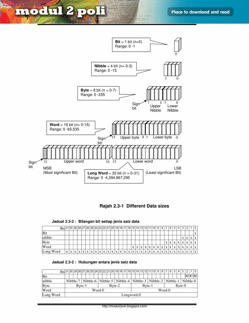
E3165 / UNIT 2 / 11
SENIBINA MIKROPEMPROSES
Rajah 2.3-1 Different Data sizes Jadual 2.3-2 : Bilangan bit setiap jenis saiz data
Jadual 2.3-2 : Hubungan antara jenis saiz data
0
0 3
0 7
0 15
0
Bit = 1 bit (n=0) Range: 0 -1
Nibble = 4 bit (n= 0-3) Range: 0 -15
Byte = 8 bit (n = 0-7) Range: 0 -255
Word = 16 bit (n= 0-15) Range: 0 -65,535
Long Word = 32 bit (n = 0-31) Range: 0 -4,294,967,295
MSB (Most significant Bit)
LSB(Least significant Bit)
Upper word Lower word
Upper byte Lower byte
Upper Nibble
Lower Nibble
Sign bit
Sign bit
31 Sign bit
4 3
7 8
15 16
Bn 31 30 29 28 27 26 25 24 23 22 21 20 19 18 17 16 15 14 13 12 11 10 9 8 7 6 5 4 3 2 1 0
Bit x
nibble x x x x
Byte x x x x x x x x
Word x x x x x x x x x x x x x x x x
Long Word x x x x x x x x x x x x x x x x x x x x x x x x x x x x x x x x
Bn 31 30 29 28 27 26 25 24 23 22 21 20 19 18 17 16 15 14 13 12 11 10 9 8 7 6 5 4 3 2 1 0
Bit B2 B1 B0
nibble Nibble-7 Nibble-6 Nibble-5 Nibble-4 Nibble-3 Nibble-2 Nibble-1 Nibble-0
Byte Byte-3 Byte-2 Byte-1 Byte-0
Word Word-0 Word-0
Long Word Longword-0
http://modul2poli.blogspot.com/
E3165 / UNIT 2 / 12
SENIBINA MIKROPEMPROSES
1 Bit = 1 bit 1 Nibble = 4 bit 1 Byte = 8 bit 1 Word = 16 bit 1 Longword = 32 bit 1 long word = 2 Word = 4 Byte = 8 Nibble = 32 Bit 1 Word = ½ Longword = 2 Byte = 4 Nibble = 16 Bit 1 Byte = ¼ Longword = ½ Word = 2 Nibble = 8 Bit 1 Nibble = 1/8 Longword = ¼ Word = ½ Byte = 4 Bit 32 Bit: 1 Nibble = 4 bit: 32 Bit = (32/4) Nibble = 8 Nibble 1 Byte = 8 bit : 32 Bit = (32/8) Byte = 4 Byte 1 Word = 16 bit : 32 Bit = (32/16) Word = 2 Word 1 Longword = 32 bit : 32 Bit = (32/32) Longword = 1 Long word 32 Bit = (32/32) LW = (32/16) Word = (32/8) Byte = (32/4) Nibble = 1 LW = 2 Word = 4 Byte = 8 Nibble 16 Bit = (16/32) LW = (16/16) Word = (16/8) Byte = (16/4) Nibble = 1/2 LW = 1 Word = 2 Byte = 4 Nibble 8 Bit = (8/32) LW = (8/16) Word = (8/8) Byte = (8/4) Nibble = 1/4 LW = 1/2 Word = 1 Byte = 2 Nibble 4 Bit = (4/32) LW = (4/16) Word = (4/8) Byte = (4/4) Nibble = 1/8 LW = 1/4 Word = 1/2 Byte = 1 Nibble 1 Bit = (1/32) LW = (1/16) Word = (1/8) Byte = (1/4) Nibble = 1/32 LW = 1/16 Word = 1/8 Byte = 1/4 Nibble Jika menilai saiz kapasiti: bilangan bit = n; kapasiti ialah = 2n.
n = 1 bit; kapasiti = 21 = 2 ; 1 bit mewakili 2 keadaan. n = 4 bit; kapasiti = 24 = 16 ; 4 bit mewakili 16 keadaan. n = 8 bit; kapasiti = 28 = 256 ; 8 bit mewakili 256 keadaan. n = 16 bit; kapasiti = 216 = 65536 ; 16 bit mewakili 65536 keadaan. n = 32 bit; kapasiti = 232 =4294967296 ; 32 bit mewakili 4294967296 keadaan. Perhatikan hubungan antara bilangan bit dengan kapasiti adalah secara eksponen. Contoh, tambahan 4 bit dari 4 ke 8, menghasilkan tambahan kapasiti 16 kali ganda (256/16). Kapasiti sesuatu sistem komputer selalunya dirujuk kepada bilangan bit yang boleh disokong. Kesimpulannya, semakin besar bilangan bit, semakin banyak maklumat dapat dikendalikan. Teknologi komputer hari ini mungkin menggunakan teknologi 64 bit, tapi esok lusa akan bertambah besar lagi.
<Unit 2.4 telah dibuang>
http://modul2poli.blogspot.com/
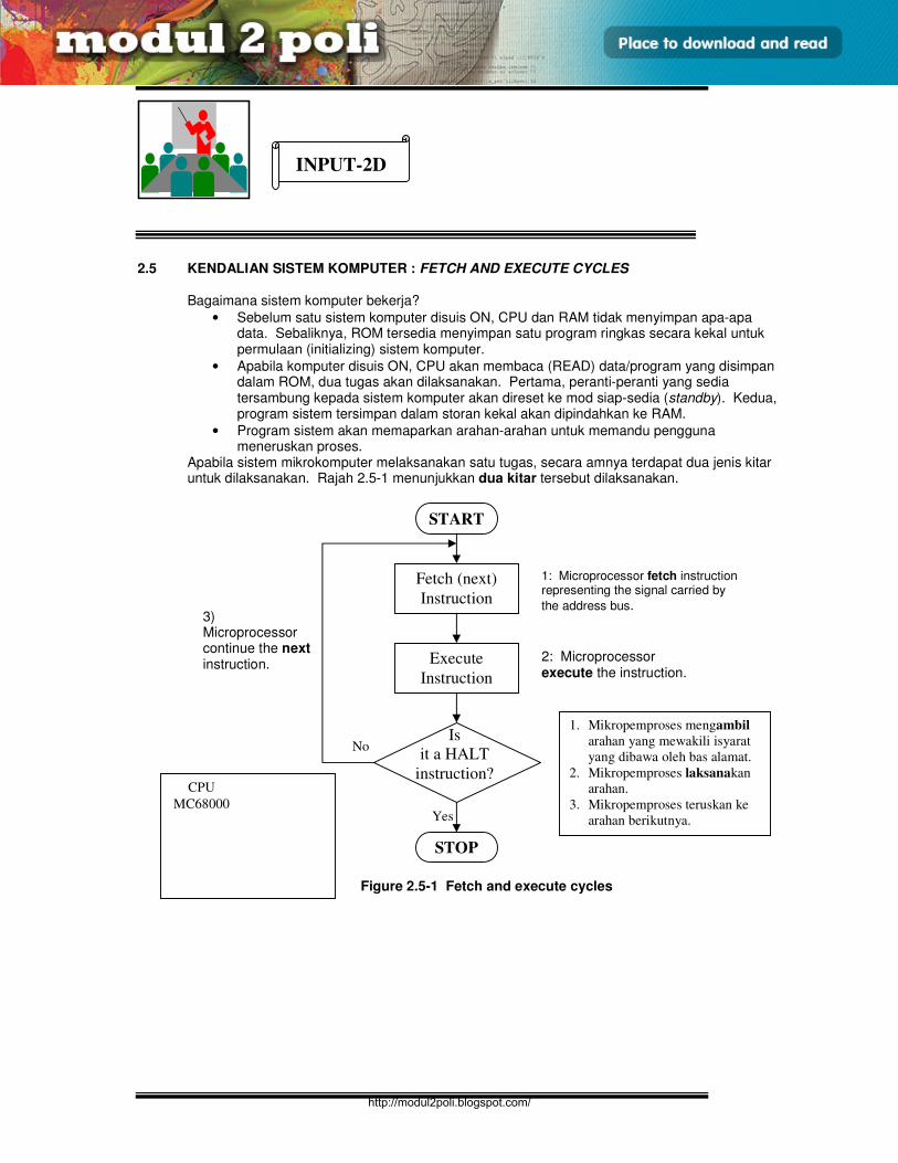
E3165 / UNIT 2 / 13
SENIBINA MIKROPEMPROSES
2.5 KENDALIAN SISTEM KOMPUTER : FETCH AND EXECUTE CYCLES
Bagaimana sistem komputer bekerja?
• Sebelum satu sistem komputer disuis ON, CPU dan RAM tidak menyimpan apa-apa data. Sebaliknya, ROM tersedia menyimpan satu program ringkas secara kekal untuk permulaan (initializing) sistem komputer.
• Apabila komputer disuis ON, CPU akan membaca (READ) data/program yang disimpan dalam ROM, dua tugas akan dilaksanakan. Pertama, peranti-peranti yang sedia tersambung kepada sistem komputer akan direset ke mod siap-sedia (standby). Kedua, program sistem tersimpan dalam storan kekal akan dipindahkan ke RAM.
• Program sistem akan memaparkan arahan-arahan untuk memandu pengguna meneruskan proses.
Apabila sistem mikrokomputer melaksanakan satu tugas, secara amnya terdapat dua jenis kitar untuk dilaksanakan. Rajah 2.5-1 menunjukkan dua kitar tersebut dilaksanakan.
INPUT-2D
1: Microprocessor fetch instruction representing the signal carried by
the address bus.
2: Microprocessor execute the instruction.
3) Microprocessor continue the next instruction.
START
Fetch (next)
Instruction
Execute
Instruction
Is
it a HALT
instruction?
STOP
Yes
No
Figure 2.5-1 Fetch and execute cycles
1. Mikropemproses mengambil
arahan yang mewakili isyarat
yang dibawa oleh bas alamat.
2. Mikropemproses laksanakan
arahan.
3. Mikropemproses teruskan ke
arahan berikutnya.
CPU
MC68000
http://modul2poli.blogspot.com/
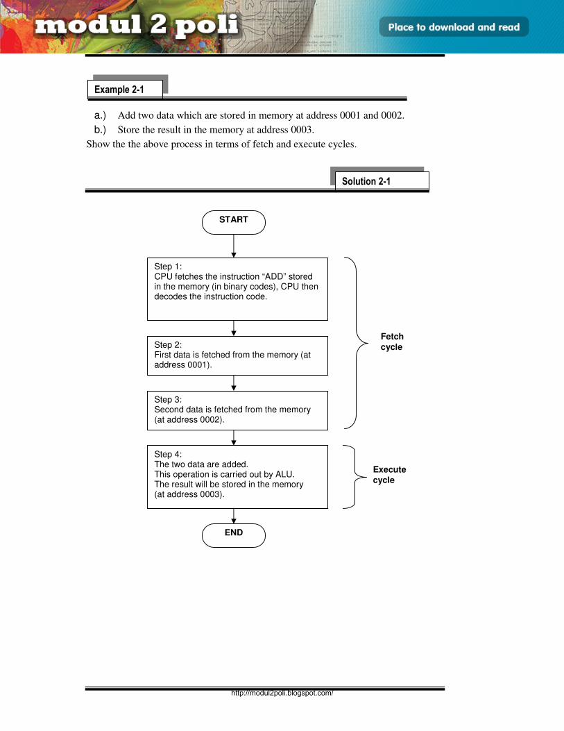
E3165 / UNIT 2 / 14
SENIBINA MIKROPEMPROSES
a.) Add two data which are stored in memory at address 0001 and 0002.
b.) Store the result in the memory at address 0003.
Show the the above process in terms of fetch and execute cycles.
Example 2-1
Solution 2-1
START
Step 1: CPU fetches the instruction “ADD” stored in the memory (in binary codes), CPU then decodes the instruction code.
Step 2: First data is fetched from the memory (at address 0001).
Step 3: Second data is fetched from the memory (at address 0002).
Step 4: The two data are added. This operation is carried out by ALU. The result will be stored in the memory (at address 0003).
END
Fetch
cycle
Execute
cycle
http://modul2poli.blogspot.com/
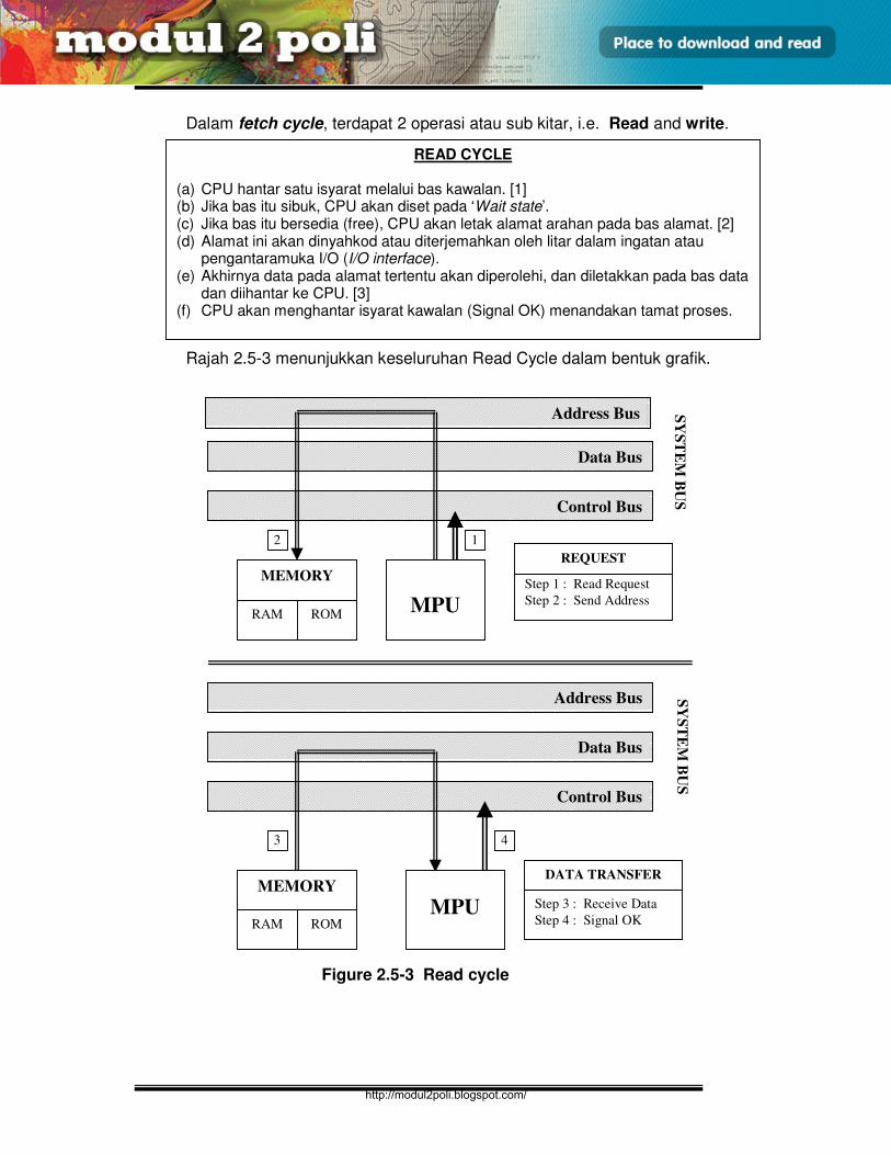
E3165 / UNIT 2 / 15
SENIBINA MIKROPEMPROSES
Dalam fetch cycle, terdapat 2 operasi atau sub kitar, i.e. Read and write.
Rajah 2.5-3 menunjukkan keseluruhan Read Cycle dalam bentuk grafik.
READ CYCLE (a) CPU hantar satu isyarat melalui bas kawalan. [1] (b) Jika bas itu sibuk, CPU akan diset pada ‘Wait state’. (c) Jika bas itu bersedia (free), CPU akan letak alamat arahan pada bas alamat. [2] (d) Alamat ini akan dinyahkod atau diterjemahkan oleh litar dalam ingatan atau
pengantaramuka I/O (I/O interface). (e) Akhirnya data pada alamat tertentu akan diperolehi, dan diletakkan pada bas data
dan diihantar ke CPU. [3] (f) CPU akan menghantar isyarat kawalan (Signal OK) menandakan tamat proses.
Figure 2.5-3 Read cycle
Address Bus
Control Bus
Data Bus
MEMORY
RAM ROM
MPU
1 2
SY
ST
EM
BU
S
Step 1 : Read Request
Step 2 : Send Address
REQUEST
Address Bus
Control Bus
Data Bus
RAM ROM
4 3
SY
ST
EM
BU
S
MEMORY
MPU Step 3 : Receive Data
Step 4 : Signal OK
DATA TRANSFER
http://modul2poli.blogspot.com/
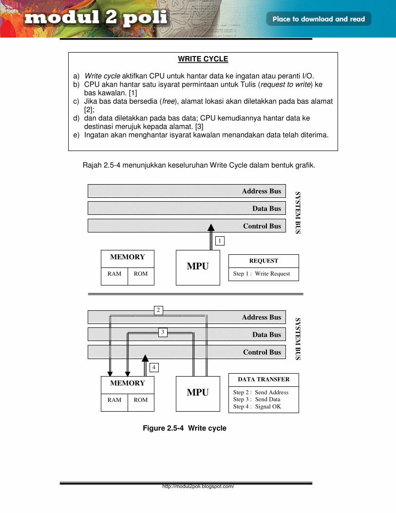
E3165 / UNIT 2 / 16
SENIBINA MIKROPEMPROSES
Rajah 2.5-4 menunjukkan keseluruhan Write Cycle dalam bentuk grafik.
WRITE CYCLE
a) Write cycle aktifkan CPU untuk hantar data ke ingatan atau peranti I/O. b) CPU akan hantar satu isyarat permintaan untuk Tulis (request to write) ke
bas kawalan. [1] c) Jika bas data bersedia (free), alamat lokasi akan diletakkan pada bas alamat
[2]; d) dan data diletakkan pada bas data; CPU kemudiannya hantar data ke
destinasi merujuk kepada alamat. [3] e) Ingatan akan menghantar isyarat kawalan menandakan data telah diterima.
Address Bus
Control Bus
Data Bus
Step 1 : Write Request
SY
ST
EM
BU
S
RAM ROM
MEMORY
MPU
1
REQUEST
Address Bus
Control Bus
Data Bus
Step 2 : Send Address
Step 3 : Send Data
Step 4 : Signal OK
SY
ST
EM
BU
S
RAM ROM
MEMORY
MPU
4
2
3
Figure 2.5-4 Write cycle
DATA TRANSFER
http://modul2poli.blogspot.com/
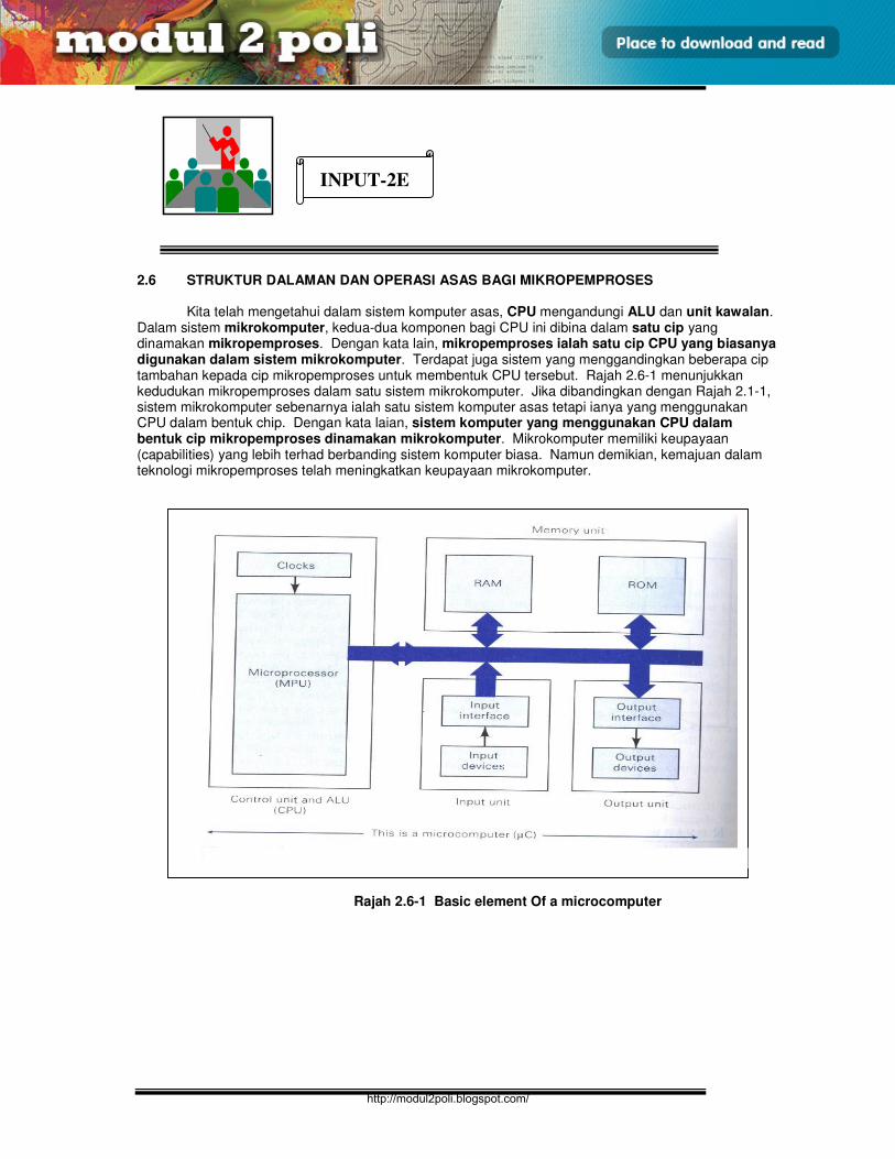
E3165 / UNIT 2 / 17
SENIBINA MIKROPEMPROSES
2.6 STRUKTUR DALAMAN DAN OPERASI ASAS BAGI MIKROPEMPROSES
Kita telah mengetahui dalam sistem komputer asas, CPU mengandungi ALU dan unit kawalan.
Dalam sistem mikrokomputer, kedua-dua komponen bagi CPU ini dibina dalam satu cip yang dinamakan mikropemproses. Dengan kata lain, mikropemproses ialah satu cip CPU yang biasanya digunakan dalam sistem mikrokomputer. Terdapat juga sistem yang menggandingkan beberapa cip tambahan kepada cip mikropemproses untuk membentuk CPU tersebut. Rajah 2.6-1 menunjukkan kedudukan mikropemproses dalam satu sistem mikrokomputer. Jika dibandingkan dengan Rajah 2.1-1, sistem mikrokomputer sebenarnya ialah satu sistem komputer asas tetapi ianya yang menggunakan CPU dalam bentuk chip. Dengan kata laian, sistem komputer yang menggunakan CPU dalam bentuk cip mikropemproses dinamakan mikrokomputer. Mikrokomputer memiliki keupayaan (capabilities) yang lebih terhad berbanding sistem komputer biasa. Namun demikian, kemajuan dalam teknologi mikropemproses telah meningkatkan keupayaan mikrokomputer.
Rajah 2.6-1 Basic element Of a microcomputer
INPUT-2E
http://modul2poli.blogspot.com/
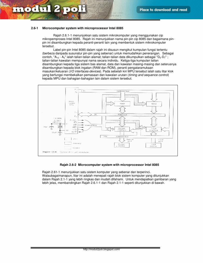
E3165 / UNIT 2 / 18
SENIBINA MIKROPEMPROSES
2.6-1 Microcomputer system with microprocessor Intel 8085
Rajah 2.6.1-1 menunjukkan satu sistem mikrokomputer yang menggunakan cip
mikropemproses Intel 8085. Rajah ini menunjukkan nama pin-pin cip 8085 dan bagaimana pin-pin ini disambungkan kepada peranti-peranti lain yang membentuk sistem mikrokomputer tersebut.
Label pin-pin Intel 8085 dalam rajah ini disusun mengikut kumpulan fungsi tertentu (berbeza daripada susunatur pin-pin yang sebenar) untuk memudahkan penerangan. Sebagai contoh, "A15 - A0" ialah talian-talian alamat; talian-talian data dikumpulkan sebagai "D0-D7" ; talian-talian kawalan mempunyai nama secara individu. Ketiga-tiga kumpulan talian disambungkan kepada tiga sistem bas alamat, data dan kawalan masing-masing dan seterusnya disambungkan kepada blok ingatan (RAM dan ROM), peranti pengataramukaan masukan/keluaran (I/O interfaces-devices). Pada sebelah kiri MPU tersebut ialah satu litar klok yang berfungsi membekalkan pemasaan dan kawalan urutan (timing and sequence control) kepada MPU dan bahagian-bahagian lain dalam sistem tersebut.
Rajah 2.6-2 Microcomputer system with microprocessor Intel 8085
Rajah 2.61-1 menunjukkan satu sistem komputer yang sebenar dan terperinci. Walaubagaimanapun, litar ini adalah menepati rajah blok sistem komputer yang ditunjukkan dalam Rajah 2.1-1 yang lebih ringkas dan mudah difahami. Untuk mendapatkan gambaran yang lebih jelas, membandingkan Rajah 2.6.1-1 dan Rajah 2.1-1 seperti ditunjukkan di bawah.
http://modul2poli.blogspot.com/
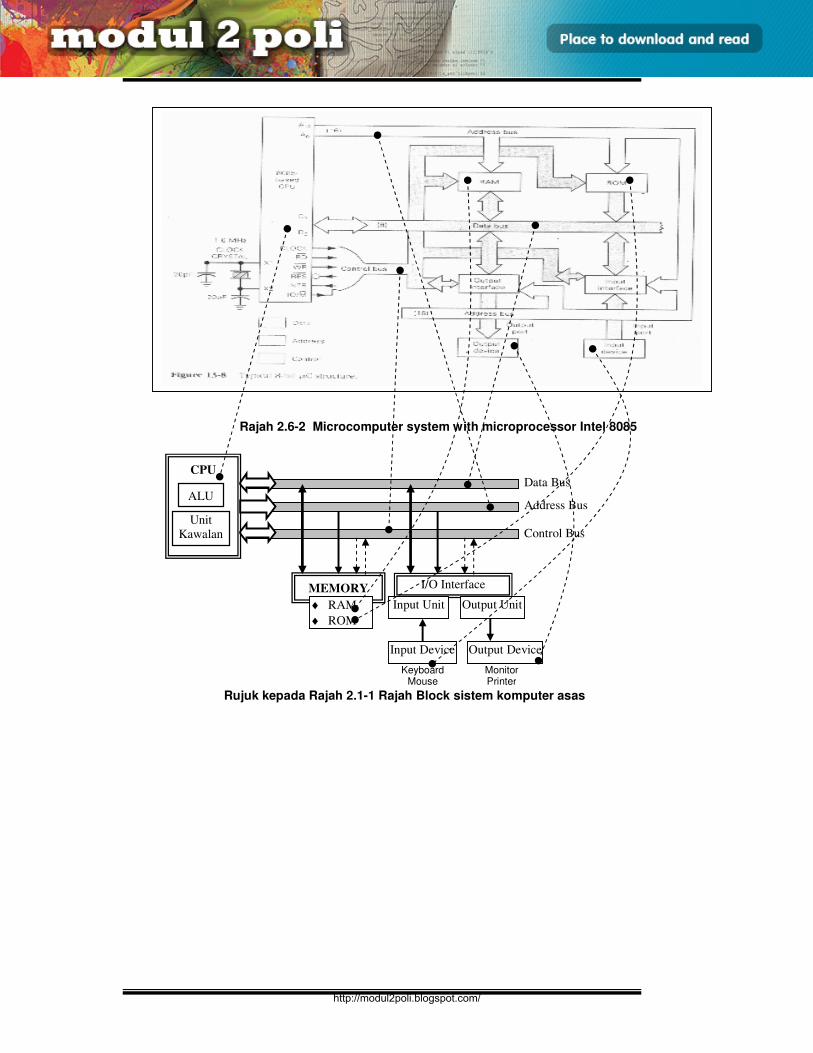
E3165 / UNIT 2 / 19
SENIBINA MIKROPEMPROSES
Rajah 2.6-2 Microcomputer system with microprocessor Intel 8085
MEMORY ♦ RAM
♦ ROM
I/O Interface
Input Unit
Data Bus
Address Bus
Control Bus
Rujuk kepada Rajah 2.1-1 Rajah Block sistem komputer asas
CPU
ALU
Unit
Kawalan
Output Unit
Input Device Output Device
Keyboard Mouse
Monitor Printer
http://modul2poli.blogspot.com/
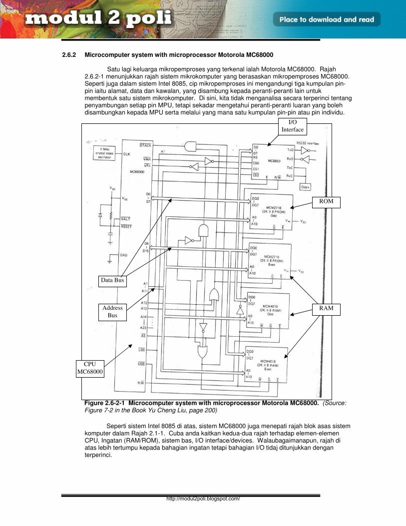
E3165 / UNIT 2 / 20
SENIBINA MIKROPEMPROSES
2.6.2 Microcomputer system with microprocessor Motorola MC68000
Satu lagi keluarga mikropemproses yang terkenal ialah Motorola MC68000. Rajah
2.6.2-1 menunjukkan rajah sistem mikrokomputer yang berasaskan mikropemproses MC68000. Seperti juga dalam sistem Intel 8085, cip mikropemproses ini mengandungi tiga kumpulan pin-pin iaitu alamat, data dan kawalan, yang disambung kepada peranti-peranti lain untuk membentuk satu sistem mikrokomputer. Di sini, kita tidak menganalisa secara terperinci tentang penyambungan setiap pin MPU, tetapi sekadar mengetahui peranti-peranti luaran yang boleh disambungkan kepada MPU serta melalui yang mana satu kumpulan pin-pin atau pin individu.
Figure 2.6-2-1 Microcomputer system with microprocessor Motorola MC68000. (Source: Figure 7-2 in the Book Yu Cheng Liu, page 200)
Seperti sistem Intel 8085 di atas, sistem MC68000 juga menepati rajah blok asas sistem
komputer dalam Rajah 2.1-1. Cuba anda kaitkan kedua-dua rajah terhadap elemen-elemen CPU, Ingatan (RAM/ROM), sistem bas, I/O interface/devices. Walaubagaimanapun, rajah di atas lebih tertumpu kepada bahagian ingatan tetapi bahagian I/O tidaj ditunjukkan dengan terperinci.
I/O
Interface
ROM
RAM
Data Bus
Address
Bus
CPU
MC68000
http://modul2poli.blogspot.com/

E3165 / UNIT 2 / 21
SENIBINA MIKROPEMPROSES
2.6.3 Pins configuration of a microprocessor chip
Seperti juga cip IC yang lain, cip mikropemproses mengandungi senibina dalaman dan disambungkan kepada persekitaran luaran melalui pin-pin yang disusun dalam satu pattern spesifik mengelilingi badan cip tersebut. Setiap pin mempunyai fungsi dan label tersendiri. Susunatur pin (pin configuration) ialah suatu rajah menunjukkan bagaimana pin-pin disusunaturkan secara fizikal. Biasanya terdapat dua bentuk rajah susunatur pin. Rajah susunatur pin yang disediakan oleh pengeluar selalunya mengikut urutan pin sebenar pada cip, manakala rajah susunatur pin untuk tujuan penerangan atau penganalisaan kendalian selalunya disusun mengikut fungsi supaya dapat memberi gambaran yang lebih jelas. Rajah 2.6.3-1 dan Rajah 2.6.3-2 menunjukkan susunatur pin-pin untuk cip µP Intel 8085 dan Motorola MC68000 microprocessor masing-masing. Terdapat banyak jenis µP, namun demikian kita akan memilih salah satu jenis iaitu Motorola MC68000 untuk diterangkan dengan terperinci seterusnya. Sebelum itu, adalah baiknya kita meneliti struktur kasar (overview) susunatur bagi perkakasan (hardware) dan perisian (software) bagi suatu sistem mikrokomputer dan pernyataan format data yang digunakan dalam pemprosesan data di dalam MC68000 microprocessor.
http://modul2poli.blogspot.com/
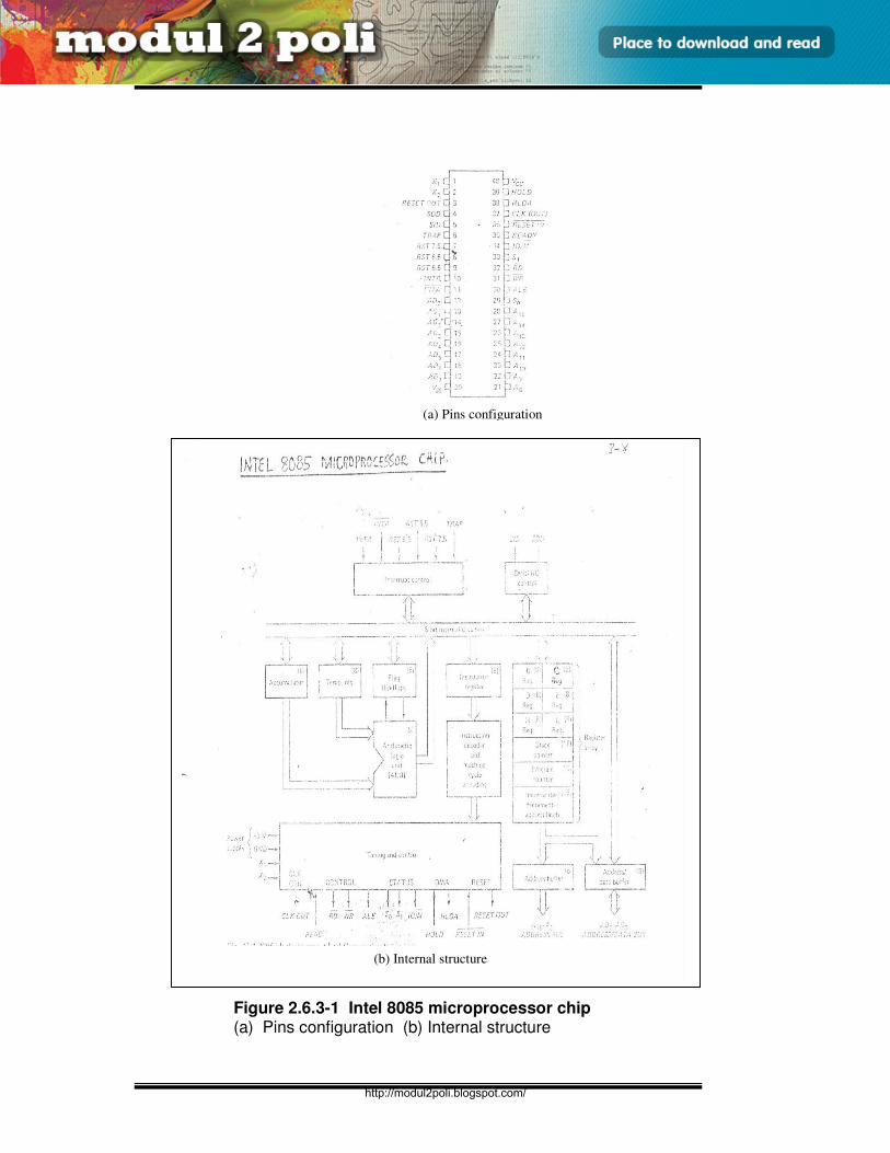
E3165 / UNIT 2 / 22
SENIBINA MIKROPEMPROSES
Figure 2.6.3-1 Intel 8085 microprocessor chip (a) Pins configuration (b) Internal structure
(a) Pins configuration
(b) Internal structure
http://modul2poli.blogspot.com/
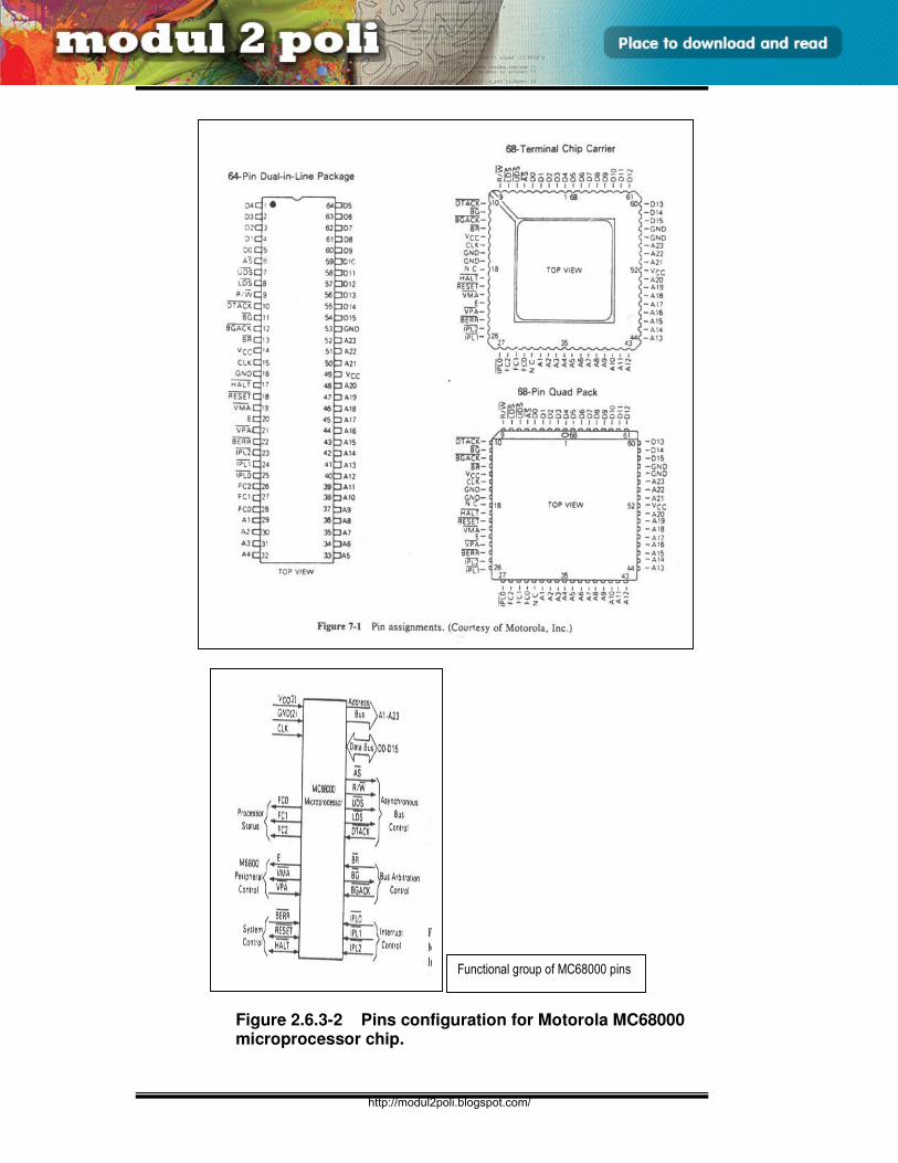
E3165 / UNIT 2 / 23
SENIBINA MIKROPEMPROSES
Figure 2.6.3-2 Pins configuration for Motorola MC68000 microprocessor chip.
Functional group of MC68000 pins
http://modul2poli.blogspot.com/
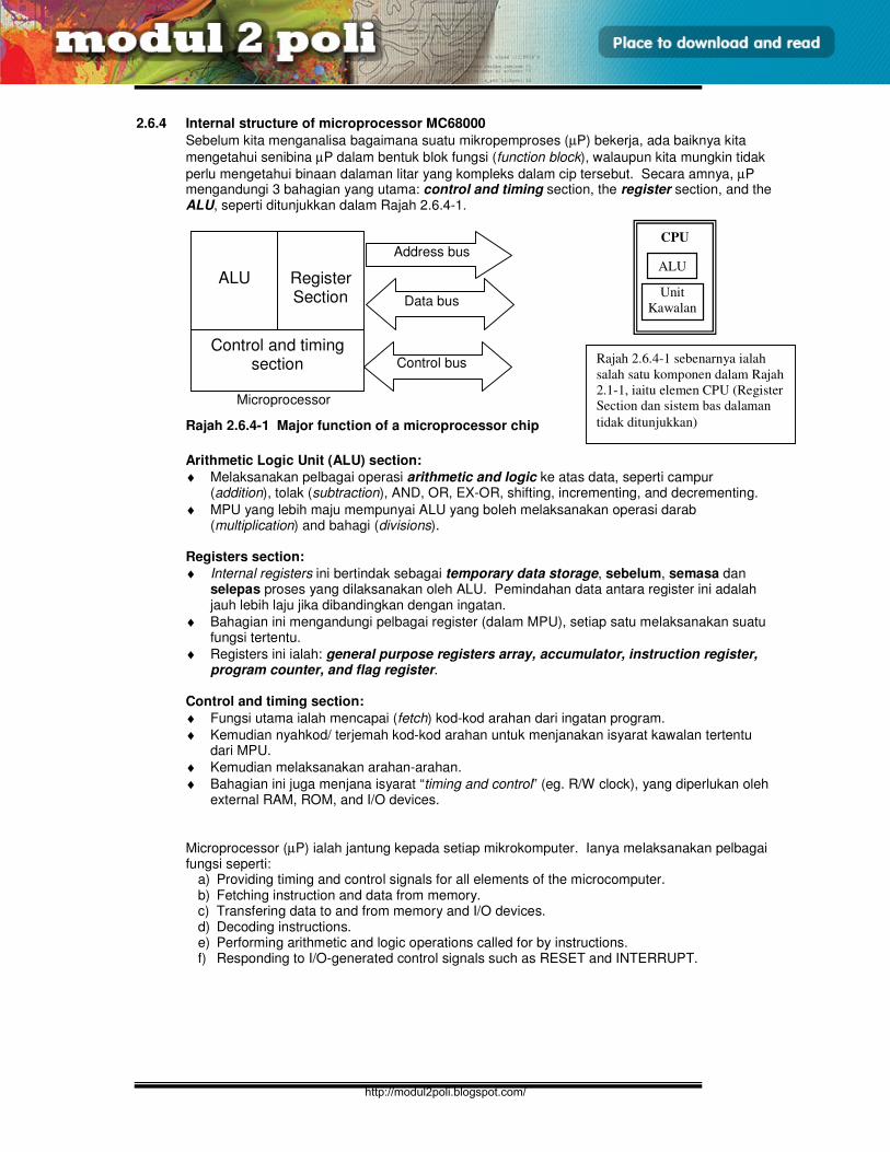
E3165 / UNIT 2 / 24
SENIBINA MIKROPEMPROSES
2.6.4 Internal structure of microprocessor MC68000
Sebelum kita menganalisa bagaimana suatu mikropemproses (µP) bekerja, ada baiknya kita
mengetahui senibina µP dalam bentuk blok fungsi (function block), walaupun kita mungkin tidak
perlu mengetahui binaan dalaman litar yang kompleks dalam cip tersebut. Secara amnya, µP mengandungi 3 bahagian yang utama: control and timing section, the register section, and the ALU, seperti ditunjukkan dalam Rajah 2.6.4-1.
Rajah 2.6.4-1 Major function of a microprocessor chip
Arithmetic Logic Unit (ALU) section:
♦ Melaksanakan pelbagai operasi arithmetic and logic ke atas data, seperti campur (addition), tolak (subtraction), AND, OR, EX-OR, shifting, incrementing, and decrementing.
♦ MPU yang lebih maju mempunyai ALU yang boleh melaksanakan operasi darab (multiplication) and bahagi (divisions).
Registers section:
♦ Internal registers ini bertindak sebagai temporary data storage, sebelum, semasa dan selepas proses yang dilaksanakan oleh ALU. Pemindahan data antara register ini adalah jauh lebih laju jika dibandingkan dengan ingatan.
♦ Bahagian ini mengandungi pelbagai register (dalam MPU), setiap satu melaksanakan suatu fungsi tertentu.
♦ Registers ini ialah: general purpose registers array, accumulator, instruction register, program counter, and flag register.
Control and timing section:
♦ Fungsi utama ialah mencapai (fetch) kod-kod arahan dari ingatan program.
♦ Kemudian nyahkod/ terjemah kod-kod arahan untuk menjanakan isyarat kawalan tertentu dari MPU.
♦ Kemudian melaksanakan arahan-arahan.
♦ Bahagian ini juga menjana isyarat “timing and control” (eg. R/W clock), yang diperlukan oleh external RAM, ROM, and I/O devices.
Microprocessor (µP) ialah jantung kepada setiap mikrokomputer. Ianya melaksanakan pelbagai fungsi seperti:
a) Providing timing and control signals for all elements of the microcomputer. b) Fetching instruction and data from memory. c) Transfering data to and from memory and I/O devices. d) Decoding instructions. e) Performing arithmetic and logic operations called for by instructions. f) Responding to I/O-generated control signals such as RESET and INTERRUPT.
ALU
Register Section
Control and timing section
Address bus
Data bus
Control bus
Microprocessor
CPU
ALU
Unit
Kawalan
Rajah 2.6.4-1 sebenarnya ialah
salah satu komponen dalam Rajah
2.1-1, iaitu elemen CPU (Register
Section dan sistem bas dalaman
tidak ditunjukkan)
http://modul2poli.blogspot.com/
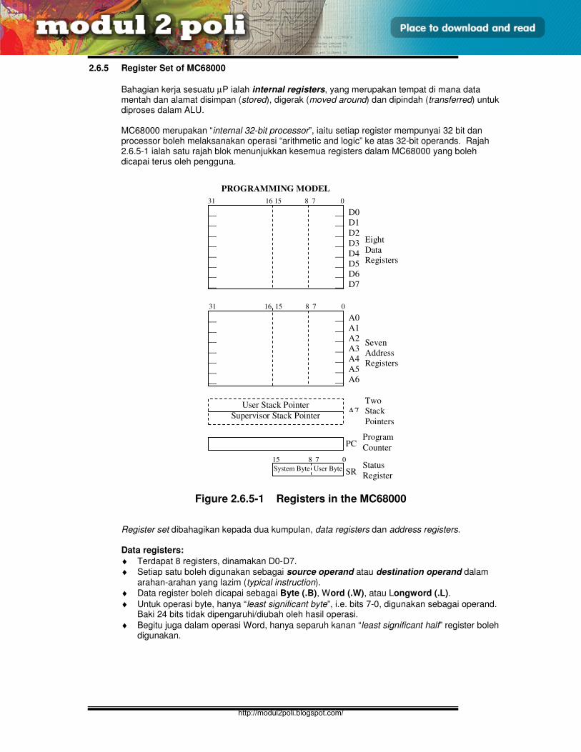
E3165 / UNIT 2 / 25
SENIBINA MIKROPEMPROSES
2.6.5 Register Set of MC68000
Bahagian kerja sesuatu µP ialah internal registers, yang merupakan tempat di mana data mentah dan alamat disimpan (stored), digerak (moved around) dan dipindah (transferred) untuk diproses dalam ALU. MC68000 merupakan “internal 32-bit processor”, iaitu setiap register mempunyai 32 bit dan processor boleh melaksanakan operasi “arithmetic and logic” ke atas 32-bit operands. Rajah 2.6.5-1 ialah satu rajah blok menunjukkan kesemua registers dalam MC68000 yang boleh dicapai terus oleh pengguna.
Register set dibahagikan kepada dua kumpulan, data registers dan address registers. Data registers:
♦ Terdapat 8 registers, dinamakan D0-D7.
♦ Setiap satu boleh digunakan sebagai source operand atau destination operand dalam arahan-arahan yang lazim (typical instruction).
♦ Data register boleh dicapai sebagai Byte (.B), Word (.W), atau Longword (.L).
♦ Untuk operasi byte, hanya “least significant byte”, i.e. bits 7-0, digunakan sebagai operand. Baki 24 bits tidak dipengaruhi/diubah oleh hasil operasi.
♦ Begitu juga dalam operasi Word, hanya separuh kanan “least significant half” register boleh digunakan.
__ D0
__ D1
__ D2
__ D3
__ D4
__ D5
__ D6
__ D7
__
__
__
__
__
__
__
__
31 16 15 8 7 0
Eight
Data
Registers
__ A0
__ A1
__ A2
__ A3
__ A4
__ A5
__ A6
__
__
__
__
__
__
__
31 16 15 8 7 0
Seven
Address
Registers
User Stack Pointer
Supervisor Stack Pointer A7
Two
Stack
Pointers
PC Program
Counter
System Byte User Byte SR Status
Register
15 8 7 0
PROGRAMMING MODEL
Figure 2.6.5-1 Registers in the MC68000
http://modul2poli.blogspot.com/

E3165 / UNIT 2 / 26
SENIBINA MIKROPEMPROSES
Address registers:
♦ Address registers, tugas utama ialah menjana alamat operand ingatan “memory operand addresses”. Oleh itu, capaian (accesses) address registers adalah lebih terhad berbanding data registers.
♦ 9 address registers, dilabel sebagai A0-A7, di mana A7 mengandungi 2 registers yang juga bertindak sebagai Stack Pointer (either SSP or the USP).
♦ Address register tidak boleh dirujuk sebagai satu byte operand.
♦ Apabila suatu operand dinyatakan sebagai source, maka address register tersebut boleh dicapai sebagai word operand (its lower 16 bits) atau longword operand.
♦ Tetapi jika digunakan sebagai destination dalam operasi word, “operand word” ialah “sign-extended” menjadi suatu longword sebelum disimpan dalam “destination address register”.
♦ Ini bermakna keseluruhan register akan dipengaruhi tanpa mengira samada saiz operasi tersebut dalam Word atau Longword.
♦ Walaupun ‘program counter’ dan ‘address registers’ mempunyai 32 bits long, hanya 24 bit rendah (lower 24 bits) digunakan untuk mengalamatkan ingatan. Ini menghadkan ruang pengaturcaraan kepada 16 megabytes.
Stack Pointer (SP):
♦ Address register A7 juga berfungsi sebagai SP samaada ‘supervisor stack pointer’ (SSP) atau ‘user stack pointer’ (USP), bergantung kepada ‘supervisor bit’ dalam ‘status register’.
♦ Dalam ‘subroutine call’ atau arahan-arahan yang lain, ‘active system SP’ digunakan secara automatik untuk ‘saving and restoring’ ‘return address’ dan lain-lain maklumat.
♦ ‘Active system SP’ ialah SSP dalam ‘supervisor mode’ dan USP dalam ‘user mode’. Program counter (PC):
♦ PC selalu menunjuk (points to) arahan yang akan dilaksanakan seterusnya.
♦ Tidak seperti ‘general purpose register’ PC tidak boleh dirujuk terus sebagai satu operand dalam sebarang arahan kecuali sebagai ‘index register’.
♦ Dalam arahan jenis ‘branch’, ‘destination’ akan dimuatkan ke PC.
♦ Untuk lain-lain arahan, kandungan PC akan ditambah (incremented) dengan panjang arahan (instruction length) semasa arahan dilaksanakan.
Status Register (SR):
♦ ‘Status register’ (SR) mempunyai 16 bits dan dibahagikan kepada ‘system byte’ dan ‘user byte’.
♦ ‘User byte’ mengandungi 5 bendera kedudukan (condition flags). Baki 3 bit tidak digunakan dan dikekalkan sifar.
♦ ‘Condition flags’ mengandungi maklumat terhadap hasil kendalian processor yang terkini/terakhir. ‘Setting’ boleh diuji dengan ‘conditional branch instructions’.
♦ Oleh kerana setiap bit bagi ‘condition flags register’ mempunyai maksud tersendiri, oleh itu satu penganalisaan terperinci adalah perlu dan dibincangkan dalam unit/bab seterusnya.
http://modul2poli.blogspot.com/
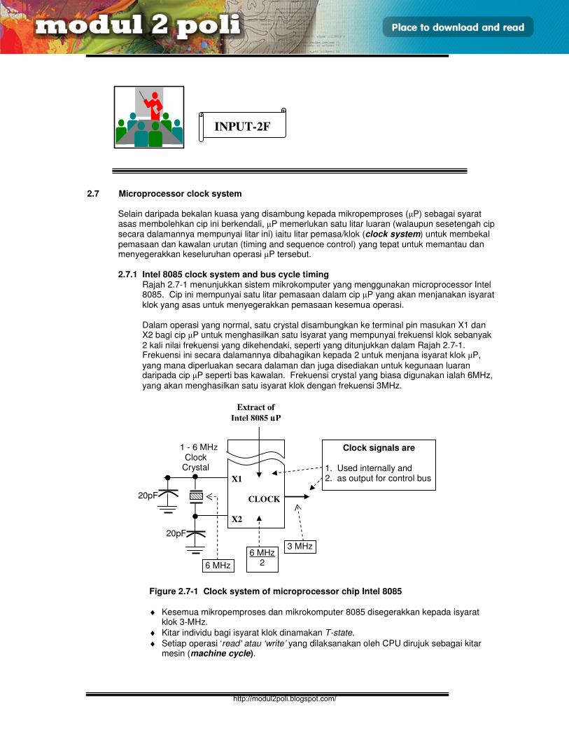
E3165 / UNIT 2 / 27
SENIBINA MIKROPEMPROSES
2.7 Microprocessor clock system
Selain daripada bekalan kuasa yang disambung kepada mikropemproses (µP) sebagai syarat asas membolehkan cip ini berkendali, µP memerlukan satu litar luaran (walaupun sesetengah cip secara dalamannya mempunyai litar ini) iaitu litar pemasa/klok (clock system) untuk membekal pemasaan dan kawalan urutan (timing and sequence control) yang tepat untuk memantau dan menyegerakkan keseluruhan operasi µP tersebut. 2.7.1 Intel 8085 clock system and bus cycle timing
Rajah 2.7-1 menunjukkan sistem mikrokomputer yang menggunakan microprocessor Intel 8085. Cip ini mempunyai satu litar pemasaan dalam cip µP yang akan menjanakan isyarat klok yang asas untuk menyegerakkan pemasaan kesemua operasi.
Dalam operasi yang normal, satu crystal disambungkan ke terminal pin masukan X1 dan X2 bagi cip µP untuk menghasilkan satu isyarat yang mempunyai frekuensi klok sebanyak 2 kali nilai frekuensi yang dikehendaki, seperti yang ditunjukkan dalam Rajah 2.7-1. Frekuensi ini secara dalamannya dibahagikan kepada 2 untuk menjana isyarat klok µP,
yang mana diperluakan secara dalaman dan juga disediakan untuk kegunaan luaran daripada cip µP seperti bas kawalan. Frekuensi crystal yang biasa digunakan ialah 6MHz, yang akan menghasilkan satu isyarat klok dengan frekuensi 3MHz.
♦ Kesemua mikropemproses dan mikrokomputer 8085 disegerakkan kepada isyarat klok 3-MHz.
♦ Kitar individu bagi isyarat klok dinamakan T-state.
♦ Setiap operasi ‘read’ atau ‘write’ yang dilaksanakan oleh CPU dirujuk sebagai kitar mesin (machine cycle).
X1
CLOCK
X2
20pF
20pF
1 - 6 MHzClock
Crystal
Extract of
Intel 8085 µµµµP
3 MHz
6 MHz
6 MHz 2
Clock signals are
1. Used internally and 2. as output for control bus
Figure 2.7-1 Clock system of microprocessor chip Intel 8085
INPUT-2F
http://modul2poli.blogspot.com/
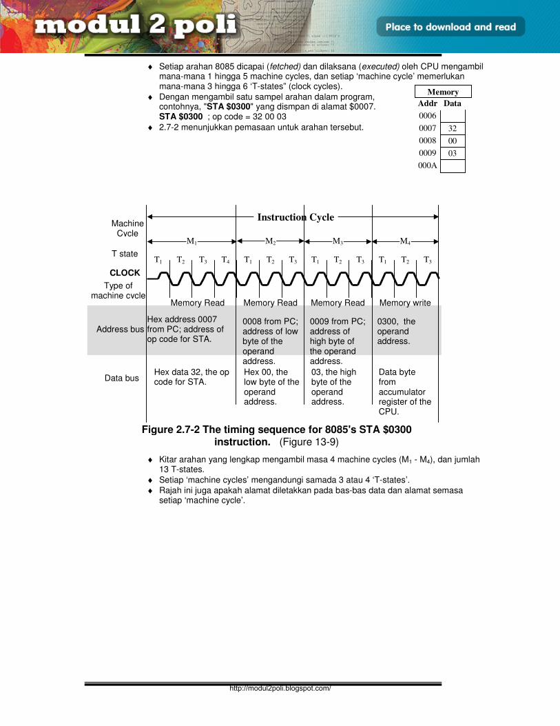
E3165 / UNIT 2 / 28
SENIBINA MIKROPEMPROSES
♦ Setiap arahan 8085 dicapai (fetched) dan dilaksana (executed) oleh CPU mengambil mana-mana 1 hingga 5 machine cycles, dan setiap ‘machine cycle’ memerlukan mana-mana 3 hingga 6 ‘T-states” (clock cycles).
♦ Dengan mengambil satu sampel arahan dalam program, contohnya, "STA $0300" yang dismpan di alamat $0007.
STA $0300 ; op code = 32 00 03
♦ 2.7-2 menunjukkan pemasaan untuk arahan tersebut.
♦ Kitar arahan yang lengkap mengambil masa 4 machine cycles (M1 - M4), dan jumlah 13 T-states.
♦ Setiap ‘machine cycles’ mengandungi samada 3 atau 4 ‘T-states’.
♦ Rajah ini juga apakah alamat diletakkan pada bas-bas data dan alamat semasa setiap ‘machine cycle’.
Address bus
Type of machine cycle
T1 T2 T3 T4 T1 T2 T3 T1 T2 T3 T1 T2 T3
M2 M3 M4 M1
Instruction Cycle
Memory Read Memory Read Memory Read Memory write
Hex address 0007 from PC; address of op code for STA.
0008 from PC; address of low byte of the operand address.
0009 from PC; address of high byte of the operand address.
0300, the operand address.
Hex data 32, the op code for STA.
Hex 00, the low byte of the operand address.
03, the high byte of the operand address.
Data byte from accumulator register of the CPU.
Data bus
CLOCK
T state
Machine Cycle
Figure 2.7-2 The timing sequence for 8085's STA $0300 instruction. (Figure 13-9)
000A
32 0007
00 0008
03 0009
0006
Data Addr
Memory
http://modul2poli.blogspot.com/
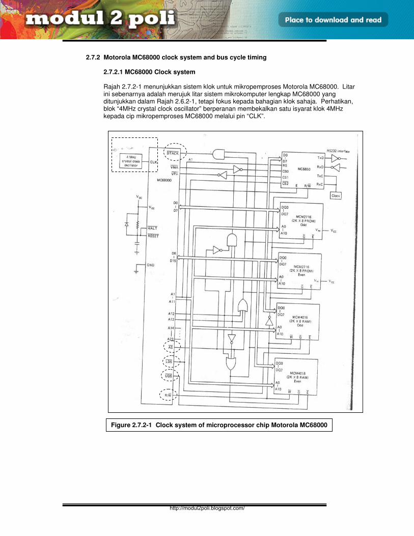
E3165 / UNIT 2 / 29
SENIBINA MIKROPEMPROSES
2.7.2 Motorola MC68000 clock system and bus cycle timing
2.7.2.1 MC68000 Clock system Rajah 2.7.2-1 menunjukkan sistem klok untuk mikropemproses Motorola MC68000. Litar ini sebenarnya adalah merujuk litar sistem mikrokomputer lengkap MC68000 yang ditunjukkan dalam Rajah 2.6.2-1, tetapi fokus kepada bahagian klok sahaja. Perhatikan, blok “4MHz crystal clock oscillator” berperanan membekalkan satu isyarat klok 4MHz kepada cip mikropemproses MC68000 melalui pin “CLK”.
Figure 2.7.2-1 Clock system of microprocessor chip Motorola MC68000
http://modul2poli.blogspot.com/
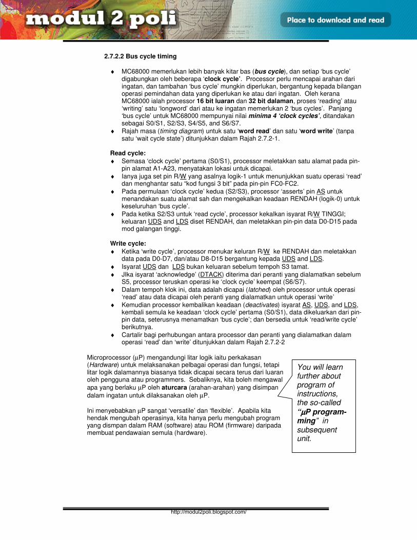
E3165 / UNIT 2 / 30
SENIBINA MIKROPEMPROSES
2.7.2.2 Bus cycle timing
♦ MC68000 memerlukan lebih banyak kitar bas (bus cycle), dan setiap ‘bus cycle’ digabungkan oleh beberapa ‘clock cycle’. Processor perlu mencapai arahan dari ingatan, dan tambahan ‘bus cycle’ mungkin diperlukan, bergantung kepada bilangan operasi pemindahan data yang diperlukan ke atau dari ingatan. Oleh kerana MC68000 ialah processor 16 bit luaran dan 32 bit dalaman, proses ‘reading’ atau ‘writing’ satu ‘longword’ dari atau ke ingatan memerlukan 2 ‘bus cycles’. Panjang ‘bus cycle’ untuk MC68000 mempunyai nilai minima 4 ‘clock cycles’, ditandakan sebagai S0/S1, S2/S3, S4/S5, and S6/S7.
♦ Rajah masa (timing diagram) untuk satu ‘word read’ dan satu ‘word write’ (tanpa satu ‘wait cycle state’) ditunjukkan dalam Rajah 2.7.2-1.
Read cycle:
♦ Semasa ‘clock cycle’ pertama (S0/S1), processor meletakkan satu alamat pada pin-pin alamat A1-A23, menyatakan lokasi untuk dicapai.
♦ Ianya juga set pin R/W yang asalnya logik-1 untuk menunjukkan suatu operasi ‘read’ dan menghantar satu “kod fungsi 3 bit” pada pin-pin FC0-FC2.
♦ Pada permulaan ‘clock cycle’ kedua (S2/S3), processor ‘asserts’ pin AS untuk menandakan suatu alamat sah dan mengekalkan keadaan RENDAH (logik-0) untuk keseluruhan ‘bus cycle’.
♦ Pada ketika S2/S3 untuk ‘read cycle’, processor kekalkan isyarat R/W TINGGI; keluaran UDS and LDS diset RENDAH, dan meletakkan pin-pin data D0-D15 pada mod galangan tinggi.
Write cycle:
♦ Ketika ‘write cycle’, processor menukar keluran R/W ke RENDAH dan meletakkan data pada D0-D7, dan/atau D8-D15 bergantung kepada UDS and LDS.
♦ Isyarat UDS dan LDS bukan keluaran sebelum tempoh S3 tamat.
♦ JIka isyarat ‘acknowledge’ (DTACK) diterima dari peranti yang dialamatkan sebelum S5, processor teruskan operasi ke ‘clock cycle’ keempat (S6/S7).
♦ Dalam tempoh klok ini, data adalah dicapai (latched) oleh processor untuk operasi ‘read’ atau data dicapai oleh peranti yang dialamatkan untuk operasi ‘write’
♦ Kemudian processor kembalikan keadaan (deactivates) isyarat AS, UDS, and LDS, kembali semula ke keadaan ‘clock cycle’ pertama (S0/S1), data dikeluarkan dari pin-pin data, seterusnya menamatkan ‘bus cycle’; dan bersedia untuk ‘read/write cycle’ berikutnya.
♦ Cartalir bagi perhubungan antara processor dan peranti yang dialamatkan dalam operasi ‘read’ dan ‘write’ ditunjukkan dalam Rajah 2.7.2-2
Microprocessor (µP) mengandungi litar logik iaitu perkakasan (Hardware) untuk melaksanakan pelbagai operasi dan fungsi, tetapi litar logik dalamannya biasanya tidak dicapai secara terus dari luaran oleh pengguna atau programmers. Sebaliknya, kita boleh mengawal
apa yang berlaku µP oleh aturcara (arahan-arahan) yang disimpan
dalam ingatan untuk dilaksanakan oleh µP.
Ini menyebabkan µP sangat ‘versatile’ dan ‘flexible’. Apabila kita hendak mengubah operasinya, kita hanya perlu mengubah program yang dismpan dalam RAM (software) atau ROM (firmware) daripada membuat pendawaian semula (hardware).
You will learn further about program of instructions, the so-called
“µµµµP program-ming” in subsequent unit.
http://modul2poli.blogspot.com/
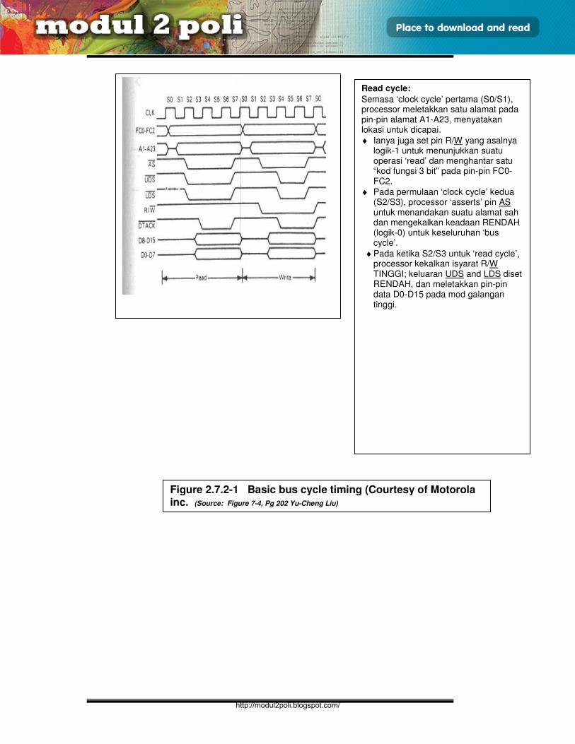
E3165 / UNIT 2 / 31
SENIBINA MIKROPEMPROSES
Figure 2.7.2-1 Basic bus cycle timing (Courtesy of Motorola inc. (Source: Figure 7-4, Pg 202 Yu-Cheng Liu)
Read cycle:
Semasa ‘clock cycle’ pertama (S0/S1), processor meletakkan satu alamat pada pin-pin alamat A1-A23, menyatakan lokasi untuk dicapai.
♦ Ianya juga set pin R/W yang asalnya logik-1 untuk menunjukkan suatu operasi ‘read’ dan menghantar satu “kod fungsi 3 bit” pada pin-pin FC0-FC2.
♦ Pada permulaan ‘clock cycle’ kedua (S2/S3), processor ‘asserts’ pin AS untuk menandakan suatu alamat sah dan mengekalkan keadaan RENDAH (logik-0) untuk keseluruhan ‘bus cycle’.
♦ Pada ketika S2/S3 untuk ‘read cycle’, processor kekalkan isyarat R/W TINGGI; keluaran UDS and LDS diset RENDAH, dan meletakkan pin-pin data D0-D15 pada mod galangan tinggi.
http://modul2poli.blogspot.com/
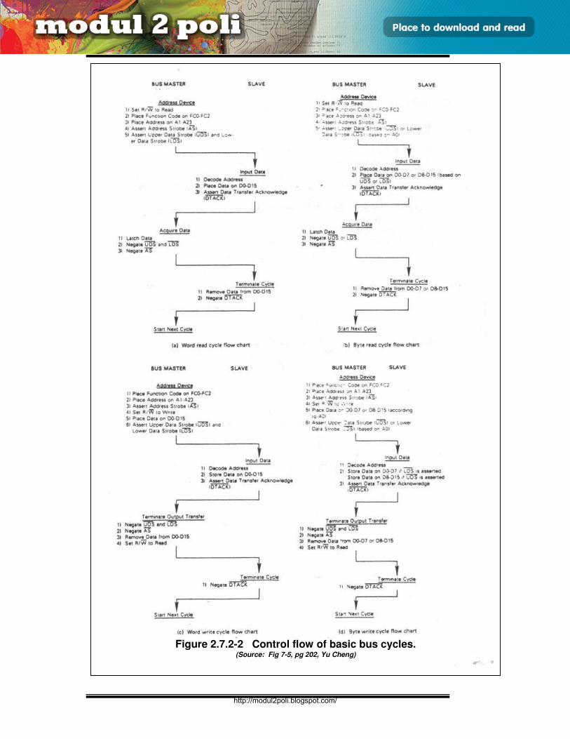
E3165 / UNIT 2 / 32
SENIBINA MIKROPEMPROSES
Figure 2.7.2-2 Control flow of basic bus cycles. (Source: Fig 7-5, pg 202, Yu Cheng)
http://modul2poli.blogspot.com/
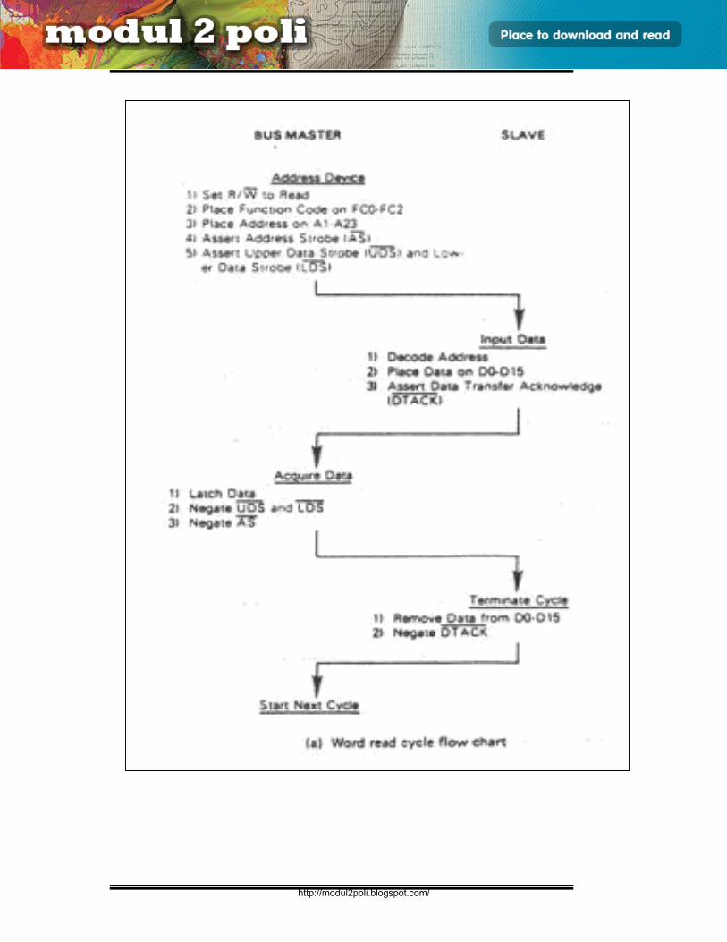
E3165 / UNIT 2 / 33
SENIBINA MIKROPEMPROSES
http://modul2poli.blogspot.com/
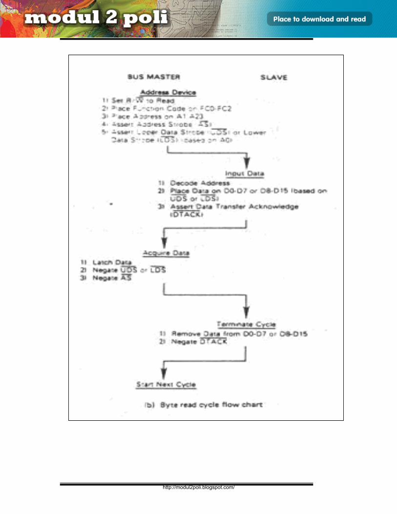
E3165 / UNIT 2 / 34
SENIBINA MIKROPEMPROSES
http://modul2poli.blogspot.com/
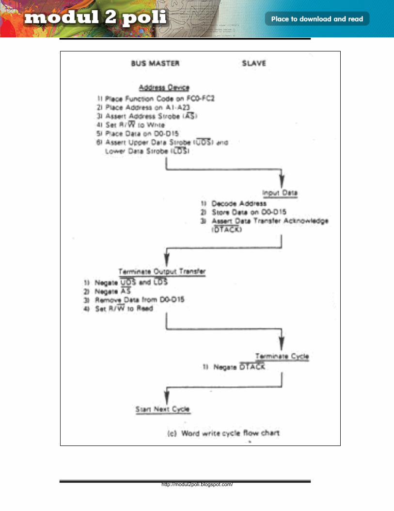
E3165 / UNIT 2 / 35
SENIBINA MIKROPEMPROSES
http://modul2poli.blogspot.com/
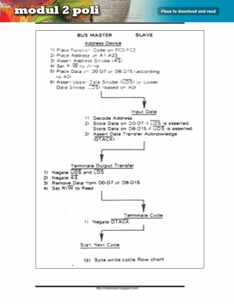
E3165 / UNIT 2 / 36
SENIBINA MIKROPEMPROSES
http://modul2poli.blogspot.com/
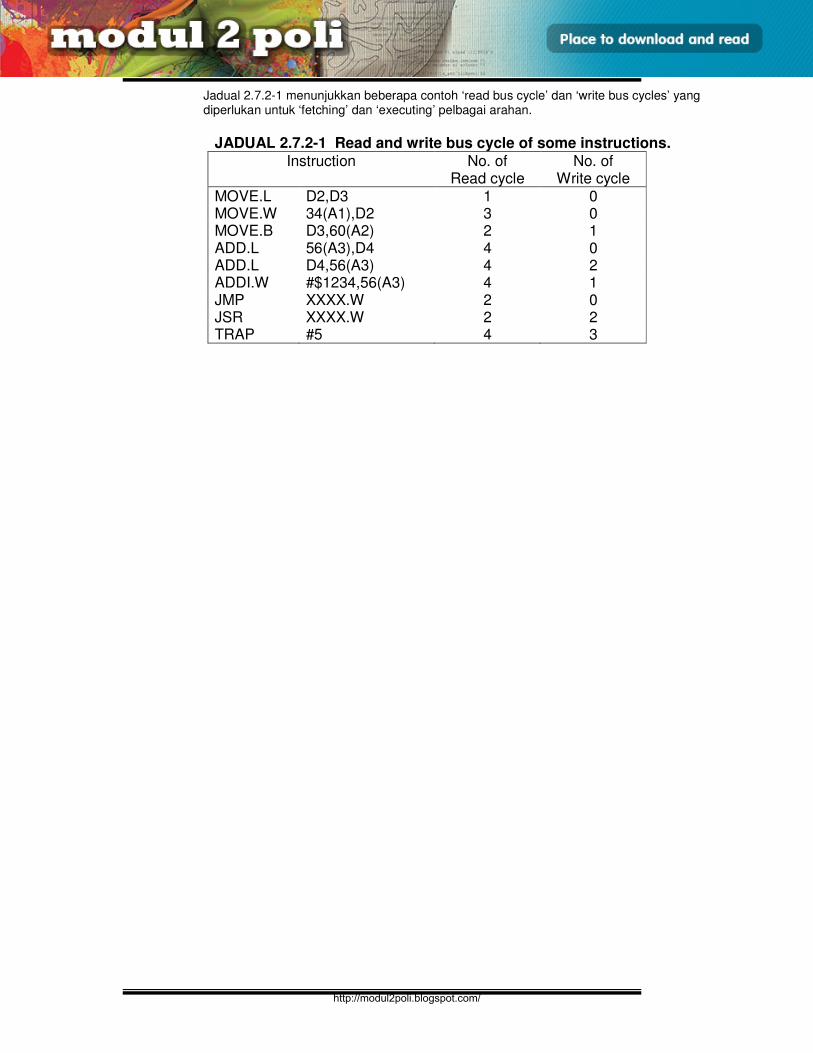
E3165 / UNIT 2 / 37
SENIBINA MIKROPEMPROSES
Jadual 2.7.2-1 menunjukkan beberapa contoh ‘read bus cycle’ dan ‘write bus cycles’ yang diperlukan untuk ‘fetching’ dan ‘executing’ pelbagai arahan.
JADUAL 2.7.2-1 Read and write bus cycle of some instructions.
Instruction No. of Read cycle
No. of Write cycle
MOVE.L D2,D3 1 0 MOVE.W 34(A1),D2 3 0 MOVE.B D3,60(A2) 2 1 ADD.L 56(A3),D4 4 0 ADD.L D4,56(A3) 4 2 ADDI.W #$1234,56(A3) 4 1 JMP XXXX.W 2 0 JSR XXXX.W 2 2 TRAP #5 4 3
http://modul2poli.blogspot.com/
E3165 / UNIT 3 / 1
ASSEMBLY LANGUAGE
Objektif Am:
Mengetahui dan memahami bahasa penghimpun (Assembly language) (instruction
sets).
Objektif Khusus:
Pada akhir unit ini anda seharusnya dapat:
3.1 Membincangkan dan membezakan antara bahasa tahap tinggi, bahasa penghimpun dan bahasa mesin.
3.2 Mendefinisi istilah-istilah berikut: mnemonik, operasi kendalian, kod mesin, label komen, operasi pseudo, operan.
3.3 Mengklasifikasikan set arahan kepada kumpulan-kumpulan berikut: 3.3.1 pemindahan data/pergerakan data 3.3.2 operasi arithmatik 3.3.3 operasi logik 3.3.4 putaran dan anjakan. 3.3.5 Cabang 3.3.6 Tindan, penunjuk tindan 3.3.7 Penukaran dan pemindahan blok 3.3.8 Arahan mikropemproses.
3.4 Menerangkan carakerja tindan mengikut konsep LIFO & FIFO. 3.5 Menyenaraikan arahan-arahan yang bersangkutan dengan tindan. 3.6 Menerangkan fungsi daftar bendera atau daftar status. 3.7 Menerangkan perubahan kepada daftar bendera mengikut bit-bit di bawah
apabila arahan bersangkutan dilaksanakan. 3.7.1 sifar (zero flag) 3.7.2 pembawa (carry flag) 3.7.3 pariti (parity flag) 3.7.4 tanda (sign flag) 3.7.5 pembawa auxiliary (auxiliary carry flag) 3.7.6 limpah (overflow flag)
UNIT 3
OBJECTIVE
http://modul2poli.blogspot.com/
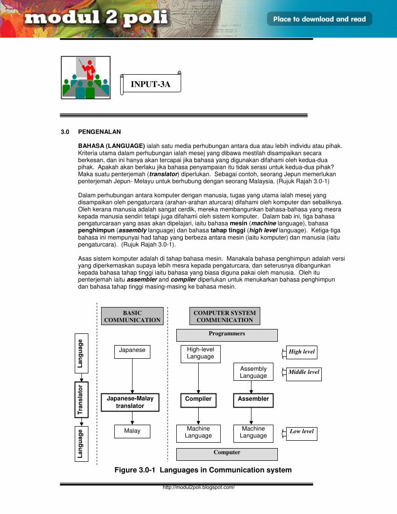
E3165 / UNIT 3 / 2
ASSEMBLY LANGUAGE
3.0 PENGENALAN
BAHASA (LANGUAGE) ialah satu media perhubungan antara dua atau lebih individu atau pihak. Kriteria utama dalam perhubungan ialah mesej yang dibawa mestilah disampaikan secara berkesan, dan ini hanya akan tercapai jika bahasa yang digunakan difahami oleh kedua-dua pihak. Apakah akan berlaku jika bahasa penyampaian itu tidak serasi untuk kedua-dua pihak? Maka suatu penterjemah (translator) diperlukan. Sebagai contoh, seorang Jepun memerlukan penterjemah Jepun- Melayu untuk berhubung dengan seorang Malaysia. (Rujuk Rajah 3.0-1) Dalam perhubungan antara komputer dengan manusia, tugas yang utama ialah mesej yang disampaikan oleh pengaturcara (arahan-arahan aturcara) difahami oleh komputer dan sebaliknya. Oleh kerana manusia adalah sangat cerdik, mereka membangunkan bahasa-bahasa yang mesra kepada manusia sendiri tetapi juga difahami oleh sistem komputer. Dalam bab ini, tiga bahasa pengaturcaraan yang asas akan dipelajari, iaitu bahasa mesin (machine language), bahasa penghimpun (assembly language) dan bahasa tahap tinggi (high level language). Ketiga-tiga bahasa ini mempunyai had tahap yang berbeza antara mesin (iaitu komputer) dan manusia (iaitu pengaturcara). (Rujuk Rajah 3.0-1). Asas sistem komputer adalah di tahap bahasa mesin. Manakala bahasa penghimpun adalah versi yang diperkemaskan supaya lebih mesra kepada pengaturcara, dan seterusnya dibangunkan kepada bahasa tahap tinggi iaitu bahasa yang biasa diguna pakai oleh manusia. Oleh itu penterjemah iaitu assembler and compiler diperlukan untuk menukarkan bahasa penghimpun dan bahasa tahap tinggi masing-masing ke bahasa mesin.
Figure 3.0-1 Languages in Communication system
INPUT-3A
Japanese-Malay
translator
Japanese
Malay
Compiler
High-level Language
Machine Language
Assembler
Assembly Language
Machine Language
High level
Middle level
Low level
Programmers
Computer
BASIC
COMMUNICATION
COMPUTER SYSTEM
COMMUNICATION
Lan
gu
ag
e
La
ng
uag
e
Tra
ns
lato
r
http://modul2poli.blogspot.com/

E3165 / UNIT 3 / 3
ASSEMBLY LANGUAGE
3.1 High level, assembly and machine languages.
Bahasa Mesin (Machine Language) Bahasa asas bagi suatu sistem komputer, biasanya dalam bentuk kod-kod binary (logic-0 atau logic-1). Bahasa ini boleh diterima(difahami) terus oleh sistem komputer.Bahasa ini lebih menghampiri komputer. Bahasa mesin jarang digunakan oleh programmer untuk menulis aturcara kerana sukar dan mudah berlaku kesilapan. Aturcara ditulis dalam bahasa penghimpun atau bahasa tahap tinggi yang kemudian diterjemah ke dalam bahasa mesin.
• Biasanya suatu sistem komputer hanya memahami bahasa mesinnya sendiri.
• Bahasa mesin ialah bahasa asas untuk sesuatu sistem komputer, yang berkait rapat dengan rekabentuk perkakasan bagi komputer berkenaan.
• Bahasa mesin biasanya mengandungi suatu pernyataan noimbor-nombor (string of numbers) atau kod-kod binari (yang akhirnya diuraikan ke bit-bit 1 atau 0), yang mengarahkan komputer untuk melaksanakan operasi yang paling asas, satu untuk satu ketika.
• Bahasa mesin ialah bergantungan kepada mesin (machine-dependant), iaitu suatu bahasa mesin hanya boleh digunakan oleh satu jenis sistem komputer sahaja, contohnya processor Intel 8085 dan Motorola 68000.
• Bahasa mesin biasanya kurang mesra/difahami oleh manusia secara amnya, Pengaturcara perlu mengetahui senibina CPU secara spesifik sesuatu sistem komputer untuk menguasai pengaturcaraan bahasa mesin.
Bahasa penghimpun (Assembly language) Bahasa pengaturcaraan yang menggunakan singkatan-singkatan (mnemonics) yang lebih miripi bahasa English (Semi English. Bahasa ini perlu ditukarkan kepada bahasa mesin menggunakan penterjemah “Assembler”. Contoh: MC68000; Intel 8085.
• Apabila komputer menjadi popular, pengaturacaraan bahasa mesin adalah dianggap terlalu perlahan dan leceh. Sebagai ganti menggunakan pernyataan nombor-nombor yang difahami secara langsung oleh komputer, pengaturcara mula menggunakan singkatan mirip bahasa Inggeris (english-like abbreviations) untuk membentuk bahasa penghimpun.
• Aturcara penterjemahan (translator program) dipanggil “assembler” telah dibangunkan untuk menukar aturcara bahasa penghimpun ke bahasa mesin pada kelajuan komputer.
• Pengaturcara perlu mengetahui senibina asas CPU seperti registers untuk menguasai pengaturcaraan bahasa penghimpun.
• Dalam seksyen berikut, kita akan mendalami bahasa penghimpun untuk salah satu mikropemproses Intel 8085 atau Motorola 68000.
Bahasa tahap tinggi (High-level language) Bahasa pengaturcaraan yang lebih mudah difahami oleh manusia dan jauh lebih mudah dan lebih cepat ditulis berbanding bahasa penghimpun menggunakan perkataan bagi bahasa biasa yang digunakan oleh manusia seperti English, Bahasa Malaysia..Contoh bahasa pengaturcaraan ialah C-Program, Visual Basic dan lain-lain. Programmer tidak perlu tahu mengenai rekabentuk dan daftar-daftar dalam mikropemproses. Bahasa ini perlu ditukarkan kepada bahasa mesin menggunakan penterjemah “Compiler”.
• Penggunaan komputer bertambah dengan mendadak berikutan terciptanya bahasa penghimpun. Namun demikian ini masih memerlukan banyak arahan untuk melaksanakan walaupun suatu tugas ringkas.
• Untuk mempercepatkan proses pengaturcaraan, bahasa tahap-tinggi telah dibangunkan di mana dengan menuliskan satu pernyataan yang ringkas mampu menyempurnakan tugas-tugas yang agak rumit.
• Aturcara penterjemahan yang menukarkan aturcara tahap-tinggi ke bahasa mesin dinamakan compilers.
• Bahasa tahap-tinggi membolehkan pengaturcara menulis arahan yang berupa perkataan Inggeris yang biasa dan juga persamaan matematik yang biasa digunakan.
• Contoh bahasa tahap-tinggi ialah Basic, Pascal, C etc.
• Pengaturcara tidak perlu mengetahui senibina CPU dalam menulis aturcara bahasa tahap-tinggi.
http://modul2poli.blogspot.com/
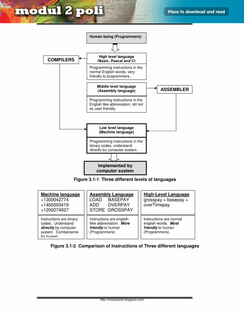
E3165 / UNIT 3 / 4
ASSEMBLY LANGUAGE
Figure 3.1-1 Three different levels of languages
Figure 3.1-2 Comparison of Instructions of Three different languages
High level language (Basic, Pascal and C)
Programming instructions in the normal English words, very friendly to programmers..
Middle level language (Assembly language)
Low level language (Machine language)
ASSEMBLER
COMPILERS
Implemented by computer system
Programming instructions in the binary codes, understand directly by computer system.
Programming instructions in the English like abbreviation, stil not so user friendly.
Human being (Programmers)
Machine language +1300042774 +1400593419 +1200274027
Assembly Language LOAD BASEPAY ADD OVERPAY STORE GROSSPAY
High-Level Language grosspay = basepay + overTimepay
Instructions are binary codes. Understand directly by computer system. Combersome for human.
Instructions are normal english words. Most friendly to human (Programmers).
Instructions are english-llike abbreviation. More friendly to human (Programmers).
http://modul2poli.blogspot.com/

E3165 / UNIT 3 / 5
ASSEMBLY LANGUAGE
Rajah 3.1-1 menunjukkan bagaimana 3 jenis bahasa pengaturcaraan dihubungkaitkan antara dua pihak utama iaitu komputer dan manusia. Perhatikan bahasa yang paling menghampiri manusia ialah bahasa tahap-tinggi manakala bahasa yang paling menghampiri komputer ialah bahasa mesin. Manusia (iaitu pengaturcara) lebih mudah menggunakan bahasa tahap tinggi (bahasa perhubungan biasa), tetapi komputer hanya memahami bahasa mesin secara semulajadi. Oleh itu bahasa penghimpun (assembly language) merupakan perantaraan untuk menggandingkan kedua-dua aras bahasa. Aturcara penterjemah (translator program) berfungsi menukarkan aturcara dari satu bahasa ke bahasa yang lain, Assembler menukar bahasa assembly ke bahasa mesin, manakala Compiler menukarkan bahasa high-level ke bahasa mesin. Pendek kata, pengaturacaraan ialah proses menyampaikan arahan manusia ke komputer secara berkesan.
Kita mengambil satu contoh aturcara ringkas untuk membandingkan ketiga-tiga bahasa pengaturcaraan: adds overtime pay to base pay and stores the result in gross pay. Campurkan “overtime pay” kepada “base pay” dan simpan hasil proses ke “gross pay”. Rajah 3.1-2 membandingkan arahan-arahan dalam tiga bahasa pengaturcaraan yang melaksanakan tugas yang sama.
http://modul2poli.blogspot.com/
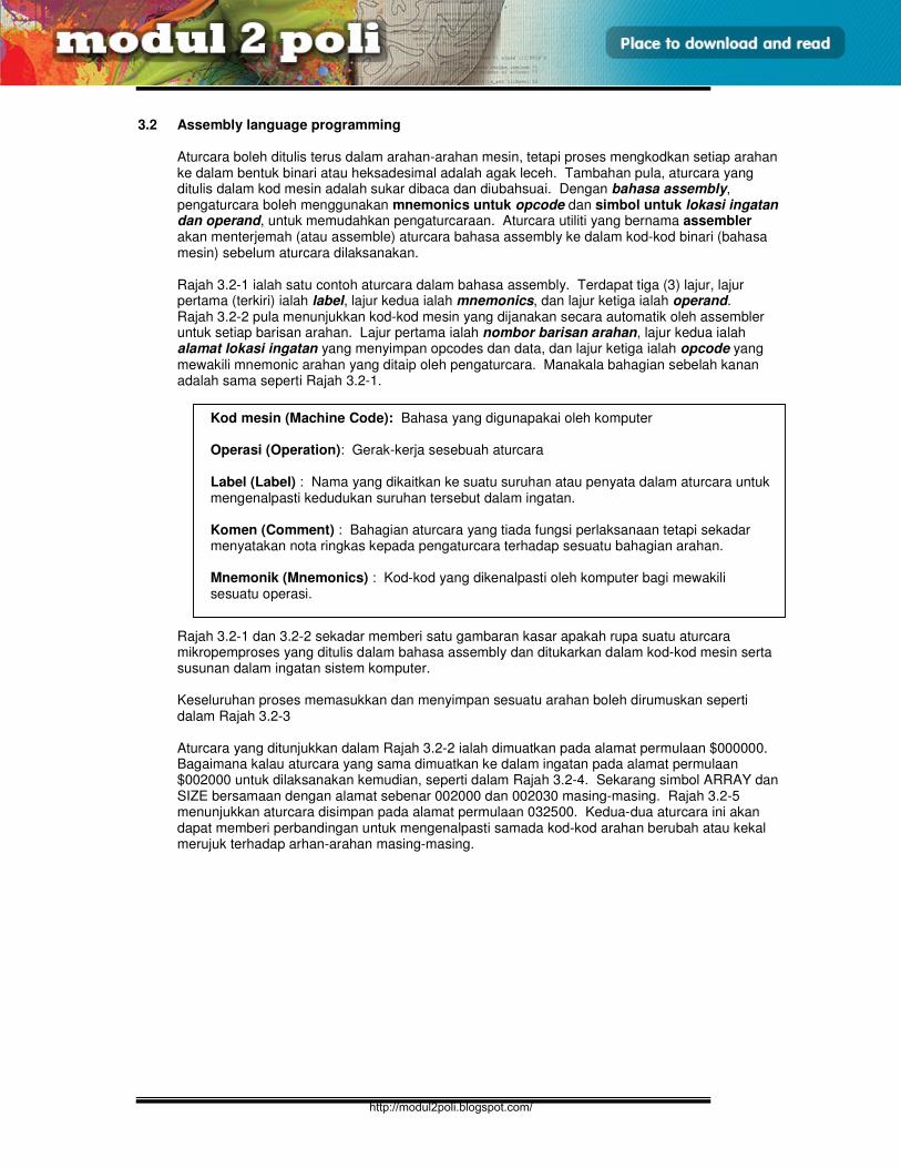
E3165 / UNIT 3 / 6
ASSEMBLY LANGUAGE
3.2 Assembly language programming
Aturcara boleh ditulis terus dalam arahan-arahan mesin, tetapi proses mengkodkan setiap arahan ke dalam bentuk binari atau heksadesimal adalah agak leceh. Tambahan pula, aturcara yang ditulis dalam kod mesin adalah sukar dibaca dan diubahsuai. Dengan bahasa assembly, pengaturcara boleh menggunakan mnemonics untuk opcode dan simbol untuk lokasi ingatan dan operand, untuk memudahkan pengaturcaraan. Aturcara utiliti yang bernama assembler akan menterjemah (atau assemble) aturcara bahasa assembly ke dalam kod-kod binari (bahasa mesin) sebelum aturcara dilaksanakan. Rajah 3.2-1 ialah satu contoh aturcara dalam bahasa assembly. Terdapat tiga (3) lajur, lajur pertama (terkiri) ialah label, lajur kedua ialah mnemonics, dan lajur ketiga ialah operand. Rajah 3.2-2 pula menunjukkan kod-kod mesin yang dijanakan secara automatik oleh assembler untuk setiap barisan arahan. Lajur pertama ialah nombor barisan arahan, lajur kedua ialah alamat lokasi ingatan yang menyimpan opcodes dan data, dan lajur ketiga ialah opcode yang mewakili mnemonic arahan yang ditaip oleh pengaturcara. Manakala bahagian sebelah kanan adalah sama seperti Rajah 3.2-1. Rajah 3.2-1 dan 3.2-2 sekadar memberi satu gambaran kasar apakah rupa suatu aturcara mikropemproses yang ditulis dalam bahasa assembly dan ditukarkan dalam kod-kod mesin serta susunan dalam ingatan sistem komputer. Keseluruhan proses memasukkan dan menyimpan sesuatu arahan boleh dirumuskan seperti dalam Rajah 3.2-3 Aturcara yang ditunjukkan dalam Rajah 3.2-2 ialah dimuatkan pada alamat permulaan $000000. Bagaimana kalau aturcara yang sama dimuatkan ke dalam ingatan pada alamat permulaan $002000 untuk dilaksanakan kemudian, seperti dalam Rajah 3.2-4. Sekarang simbol ARRAY dan SIZE bersamaan dengan alamat sebenar 002000 dan 002030 masing-masing. Rajah 3.2-5 menunjukkan aturcara disimpan pada alamat permulaan 032500. Kedua-dua aturcara ini akan dapat memberi perbandingan untuk mengenalpasti samada kod-kod arahan berubah atau kekal merujuk terhadap arhan-arahan masing-masing.
Kod mesin (Machine Code): Bahasa yang digunapakai oleh komputer Operasi (Operation): Gerak-kerja sesebuah aturcara Label (Label) : Nama yang dikaitkan ke suatu suruhan atau penyata dalam aturcara untuk mengenalpasti kedudukan suruhan tersebut dalam ingatan. Komen (Comment) : Bahagian aturcara yang tiada fungsi perlaksanaan tetapi sekadar menyatakan nota ringkas kepada pengaturcara terhadap sesuatu bahagian arahan. Mnemonik (Mnemonics) : Kod-kod yang dikenalpasti oleh komputer bagi mewakili sesuatu operasi.
http://modul2poli.blogspot.com/
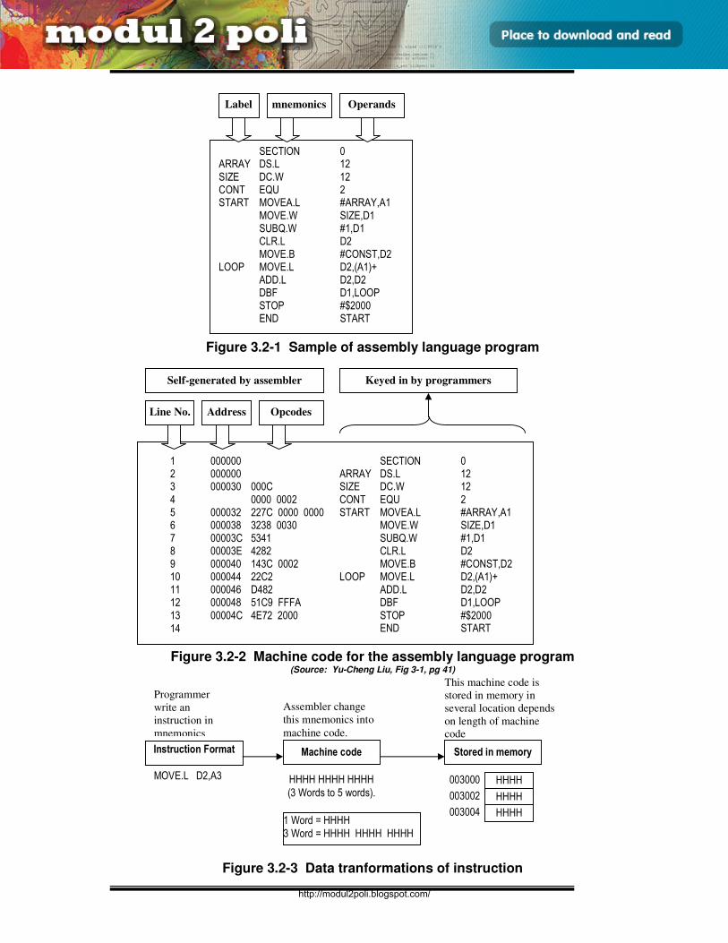
E3165 / UNIT 3 / 7
ASSEMBLY LANGUAGE
Figure 3.2-1 Sample of assembly language program
Figure 3.2-2 Machine code for the assembly language program (Source: Yu-Cheng Liu, Fig 3-1, pg 41)
Figure 3.2-3 Data tranformations of instruction
SECTION 0 ARRAY DS.L 12 SIZE DC.W 12 CONT EQU 2 START MOVEA.L #ARRAY,A1
MOVE.W SIZE,D1 SUBQ.W #1,D1 CLR.L D2 MOVE.B #CONST,D2
LOOP MOVE.L D2,(A1)+ ADD.L D2,D2 DBF D1,LOOP STOP #$2000 END START
SECTION 0 ARRAY DS.L 12 SIZE DC.W 12 CONT EQU 2 START MOVEA.L #ARRAY,A1
MOVE.W SIZE,D1 SUBQ.W #1,D1 CLR.L D2 MOVE.B #CONST,D2
LOOP MOVE.L D2,(A1)+ ADD.L D2,D2 DBF D1,LOOP STOP #$2000 END START
1 000000 2 000000 3 000030 000C 4 0000 0002 5 000032 227C 0000 0000 6 000038 3238 0030 7 00003C 5341 8 00003E 4282 9 000040 143C 0002 10 000044 22C2 11 000046 D482 12 000048 51C9 FFFA 13 00004C 4E72 2000 14
Label mnemonics Operands
Line No. Address Opcodes
Self-generated by assembler Keyed in by programmers
Programmer
write an
instruction in
mnemonics
Instruction Format
MOVE.L D2,A3
Assembler change
this mnemonics into
machine code.
Machine code
HHHH HHHH HHHH (3 Words to 5 words).
This machine code is
stored in memory in
several location depends
on length of machine
code
Stored in memory
003000 HHHH
003002 HHHH
003004 HHHH 1 Word = HHHH 3 Word = HHHH HHHH HHHH
http://modul2poli.blogspot.com/

E3165 / UNIT 3 / 8
ASSEMBLY LANGUAGE
Figure 3.2-4 Machine code for program initiated at $002000 (Source: Yu-Cheng Liu, Fig 3-2(a), pg 41)
Figure 3.2-5 Machine code for program initiated at $032500 (Source: Yu-Cheng Liu, Fig 3-2(b), pg 41)
SECTION 0 ARRAY DS.L 12 SIZE DC.W 12 CONT EQU 2 START MOVEA.L #ARRAY,A1
MOVE.W SIZE,D1 SUBQ.W #1,D1 CLR.L D2 MOVE.B #CONST,D2
LOOP MOVE.L D2,(A1)+ ADD.L D2,D2 DBF D1,LOOP STOP #$2000 END START
1 002000 2 002000 3 002030 000C 4 0000 0002 5 002032 227C 0000 2000 6 002038 3239 0000 2030 7 00003E 5341 8 000040 4282 9 000042 143C 0002 10 000046 22C2 11 000048 D482 12 00004A 51C9 FFFA 13 00004E 4E72 2000 14
SECTION 0 ARRAY DS.L 12 SIZE DC.W 12 CONT EQU 2 START MOVEA.L #ARRAY,A1
MOVE.W SIZE,D1 SUBQ.W #1,D1 CLR.L D2 MOVE.B #CONST,D2
LOOP MOVE.L D2,(A1)+ ADD.L D2,D2 DBF D1,LOOP STOP #$2000 END START
1 032500 2 032500 3 032530 000C 4 0000 0002 5 032532 227C 0003 2500 6 032538 3239 0003 2530 7 03253E 5341 8 032540 4282 9 032542 143C 0002 10 032546 22C2 11 032548 D482 12 03254A 51C9 FFFA 13 03254E 4E72 2000 14
Alamat berubah merujuk Start address
Start address
Opcode juga akan berubah merujuk
alamat semasa
Opcode juga akan berubah merujuk
alamat semasa
Opcode yang tidak melibatkan indeks alamat
akan kekal merujuk mnemonics arahan
You may understand more about Figure 3.2-4 and 3.2-5 at
the end of Chapter 3 after you have frequently assembled
the programs and stored in certain location addresses.
http://modul2poli.blogspot.com/
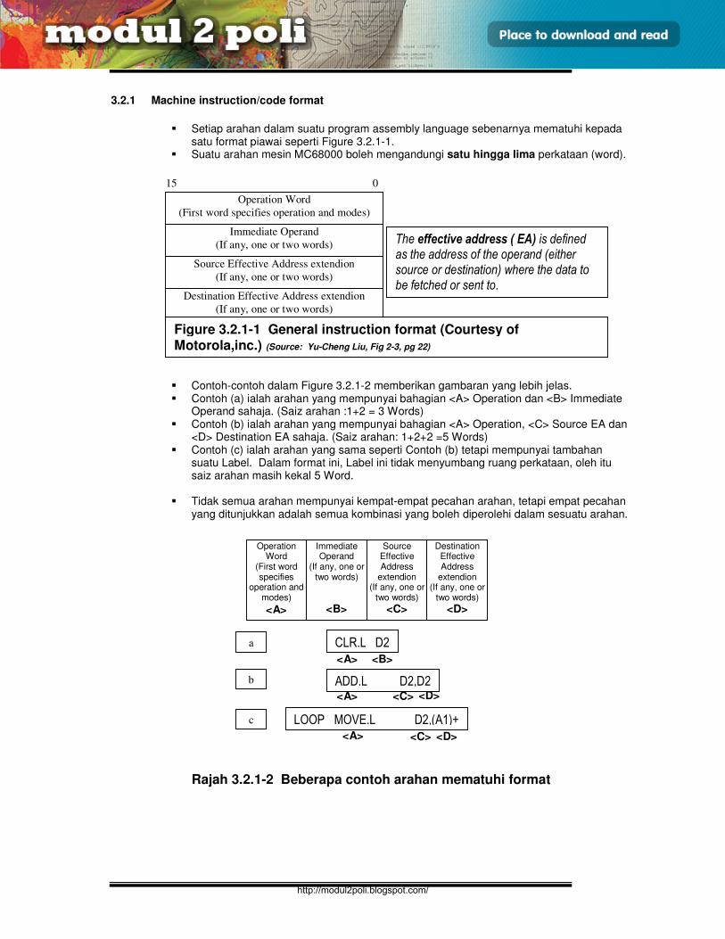
E3165 / UNIT 3 / 9
ASSEMBLY LANGUAGE
3.2.1 Machine instruction/code format
Setiap arahan dalam suatu program assembly language sebenarnya mematuhi kepada
satu format piawai seperti Figure 3.2.1-1. Suatu arahan mesin MC68000 boleh mengandungi satu hingga lima perkataan (word).
Contoh-contoh dalam Figure 3.2.1-2 memberikan gambaran yang lebih jelas. Contoh (a) ialah arahan yang mempunyai bahagian <A> Operation dan <B> Immediate
Operand sahaja. (Saiz arahan :1+2 = 3 Words) Contoh (b) ialah arahan yang mempunyai bahagian <A> Operation, <C> Source EA dan
<D> Destination EA sahaja. (Saiz arahan: 1+2+2 =5 Words) Contoh (c) ialah arahan yang sama seperti Contoh (b) tetapi mempunyai tambahan
suatu Label. Dalam format ini, Label ini tidak menyumbang ruang perkataan, oleh itu saiz arahan masih kekal 5 Word.
Tidak semua arahan mempunyai kempat-empat pecahan arahan, tetapi empat pecahan
yang ditunjukkan adalah semua kombinasi yang boleh diperolehi dalam sesuatu arahan.
Rajah 3.2.1-2 Beberapa contoh arahan mematuhi format
15 0
Operation Word
(First word specifies operation and modes)
Immediate Operand
(If any, one or two words)
Source Effective Address extendion
(If any, one or two words)
Destination Effective Address extendion
(If any, one or two words)
Figure 3.2.1-1 General instruction format (Courtesy of Motorola,inc.) (Source: Yu-Cheng Liu, Fig 2-3, pg 22)
The effective address ( EA) is defined as the address of the operand (either source or destination) where the data to be fetched or sent to.
Operation Word
(First word specifies
operation and modes)
<A>
Immediate Operand
(If any, one or two words)
<B>
Source Effective Address
extendion (If any, one or
two words)
<C>
Destination Effective Address
extendion (If any, one or
two words)
<D>
<A> <C> <D>
LOOP MOVE.L D2,(A1)+
<A> <B>
CLR.L D2
<A> <C> <D>
ADD.L D2,D2 b
c
a
http://modul2poli.blogspot.com/
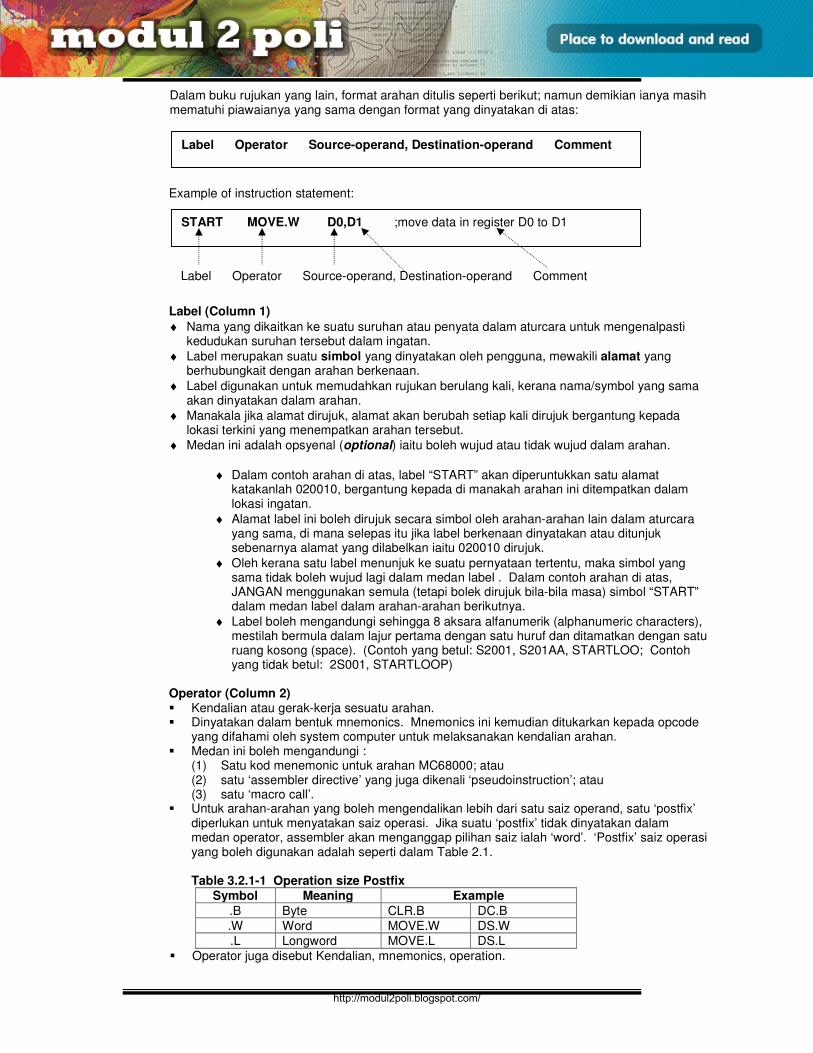
E3165 / UNIT 3 / 10
ASSEMBLY LANGUAGE
Dalam buku rujukan yang lain, format arahan ditulis seperti berikut; namun demikian ianya masih mematuhi piawaianya yang sama dengan format yang dinyatakan di atas:
Example of instruction statement:
Label (Column 1)
♦ Nama yang dikaitkan ke suatu suruhan atau penyata dalam aturcara untuk mengenalpasti kedudukan suruhan tersebut dalam ingatan.
♦ Label merupakan suatu simbol yang dinyatakan oleh pengguna, mewakili alamat yang berhubungkait dengan arahan berkenaan.
♦ Label digunakan untuk memudahkan rujukan berulang kali, kerana nama/symbol yang sama akan dinyatakan dalam arahan.
♦ Manakala jika alamat dirujuk, alamat akan berubah setiap kali dirujuk bergantung kepada lokasi terkini yang menempatkan arahan tersebut.
♦ Medan ini adalah opsyenal (optional) iaitu boleh wujud atau tidak wujud dalam arahan.
♦ Dalam contoh arahan di atas, label “START” akan diperuntukkan satu alamat katakanlah 020010, bergantung kepada di manakah arahan ini ditempatkan dalam lokasi ingatan.
♦ Alamat label ini boleh dirujuk secara simbol oleh arahan-arahan lain dalam aturcara yang sama, di mana selepas itu jika label berkenaan dinyatakan atau ditunjuk sebenarnya alamat yang dilabelkan iaitu 020010 dirujuk.
♦ Oleh kerana satu label menunjuk ke suatu pernyataan tertentu, maka simbol yang sama tidak boleh wujud lagi dalam medan label . Dalam contoh arahan di atas, JANGAN menggunakan semula (tetapi bolek dirujuk bila-bila masa) simbol “START” dalam medan label dalam arahan-arahan berikutnya.
♦ Label boleh mengandungi sehingga 8 aksara alfanumerik (alphanumeric characters), mestilah bermula dalam lajur pertama dengan satu huruf dan ditamatkan dengan satu ruang kosong (space). (Contoh yang betul: S2001, S201AA, STARTLOO; Contoh yang tidak betul: 2S001, STARTLOOP)
Operator (Column 2) Kendalian atau gerak-kerja sesuatu arahan. Dinyatakan dalam bentuk mnemonics. Mnemonics ini kemudian ditukarkan kepada opcode
yang difahami oleh system computer untuk melaksanakan kendalian arahan. Medan ini boleh mengandungi :
(1) Satu kod menemonic untuk arahan MC68000; atau (2) satu ‘assembler directive’ yang juga dikenali ‘pseudoinstruction’; atau (3) satu ‘macro call’.
Untuk arahan-arahan yang boleh mengendalikan lebih dari satu saiz operand, satu ‘postfix’ diperlukan untuk menyatakan saiz operasi. Jika suatu ‘postfix’ tidak dinyatakan dalam medan operator, assembler akan menganggap pilihan saiz ialah ‘word’. ‘Postfix’ saiz operasi yang boleh digunakan adalah seperti dalam Table 2.1. Table 3.2.1-1 Operation size Postfix
Symbol Meaning Example
.B Byte CLR.B DC.B
.W Word MOVE.W DS.W
.L Longword MOVE.L DS.L
Operator juga disebut Kendalian, mnemonics, operation.
Label Operator Source-operand, Destination-operand Comment
START MOVE.W D0,D1 ;move data in register D0 to D1
Label Operator Source-operand, Destination-operand Comment
http://modul2poli.blogspot.com/
E3165 / UNIT 3 / 11
ASSEMBLY LANGUAGE
Operand (Column 3) Merupakan subjek atau objek kepada operasi arahan. Terdiri daripada source dan Destinasion operand. Medan operand bergantung kepada operator, yang boleh mempunyai lebih daripada satu
operand. Jika terdapat dua operand, satu koma digunakan untuk memisahkannya, dengan ‘source
operand’ diikuti dengan ‘destination operand’ (Eg: ADD.W D2, XYZ; where D2 = source, XYZ = destination.)
Prosesnya boleh jadi suatu data (destination operand) dicapai dari ingatan (source operand). (Eg. MOVE.L #$30,D7), atau dicapai dari alamat ingatan bagi suatu data. (Eg. STOP #$2000)
Terdapat sebahagian arahan yang hanya mempunyai ‘opcode’, tanpa operand. (Eg. Clear, RTS).
Komen / Comment (Column 4) : Bahagian aturcara yang tiada fungsi perlaksanaan tetapi sekadar menyatakan nota ringkas kepada pengaturcara terhadap sesuatu bahagian arahan. Perhatikan contoh aturcara sebenar di Figure 3.2-1, format arahan adalah <Label> <Mnemonics> <Operand> adalah hamper sama dengan format arahan ini. <Operator> sebenarnya ialah <mnemonics> manakala Operand merangkumi Source dan Destination.
Rujuk Pg 6-4 Penyata Penghimpun (Assembler Format) Rujuk Pg 6-5 Medan Label (Label Column) Rujuk Pg 6-5 Medan Operasi (Operator Column) Rujuk Pg 6-6 Medan Kendalian (Operands Column) Rujuk Pg 6-6 Medan Komen (Comment Column) Rujuk Pg 6-7 Pemalar (Constant)
http://modul2poli.blogspot.com/
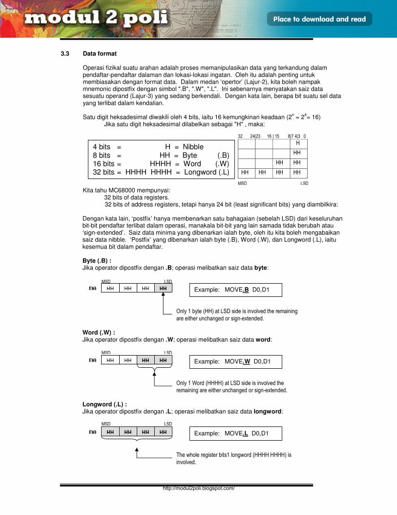
E3165 / UNIT 3 / 12
ASSEMBLY LANGUAGE
3.3 Data format
Operasi fizikal suatu arahan adalah proses memanipulasikan data yang terkandung dalam pendaftar-pendaftar dalaman dan lokasi-lokasi ingatan. Oleh itu adalah penting untuk membiasakan dengan format data. Dalam medan ‘opertor’ (Lajur-2), kita boleh nampak mnemonic dipostfix dengan simbol ".B", ".W", ".L". Ini sebenarnya menyatakan saiz data sesuatu operand (Lajur-3) yang sedang berkendali. Dengan kata lain, berapa bit suatu sel data yang terlibat dalam kendalian.
Satu digit heksadesimal diwakili oleh 4 bits, iaitu 16 kemungkinan keadaan (2
n = 2
4= 16)
Jika satu digit heksadesimal dilabelkan sebagai "H" , maka:
Kita tahu MC68000 mempunyai:
32 bits of data registers. 32 bits of address registers, tetapi hanya 24 bit (least significant bits) yang diambilkira:
Dengan kata lain, ‘postfix’ hanya membenarkan satu bahagaian (sebelah LSD) dari keseluruhan bit-bit pendaftar terlibat dalam operasi, manakala bit-bit yang lain samada tidak berubah atau ‘sign-extended’. Saiz data minima yang dibenarkan ialah byte, oleh itu kita boleh mengabaikan saiz data nibble. ‘Postfix’ yang dibenarkan ialah byte (.B), Word (.W), dan Longword (.L), iaitu kesemua bit dalam pendaftar. Byte (.B) : Jika operator dipostfix dengan .B; operasi melibatkan saiz data byte:
Word (.W) : Jika operator dipostfix dengan .W; operasi melibatkan saiz data word:
Longword (.L) : Jika operator dipostfix dengan .L; operasi melibatkan saiz data longword:
Only 1 byte (HH) at LSD side is involved the remaining are either unchanged or sign-extended.
Example: MOVE.B D0,D1
Only 1 Word (HHHH) at LSD side is involved the remaining are either unchanged or sign-extended.
Example: MOVE.W D0,D1
D0 HH HH HH HH
The whole register bits1 longword (HHHH HHHH) is involved.
Example: MOVE.L D0,D1
D0 HH HH HH HH
MSD LSD
MSD LSD
D0 HH HH HH HH
MSD LSD
4 bits = H = Nibble 8 bits = HH = Byte (.B) 16 bits = HHHH = Word (.W) 32 bits = HHHH HHHH = Longword (.L)
32 24|23 16 | 15 8|7 4|3 0
H
HH
HH HH
HH HH HH HH
MSD LSD
http://modul2poli.blogspot.com/
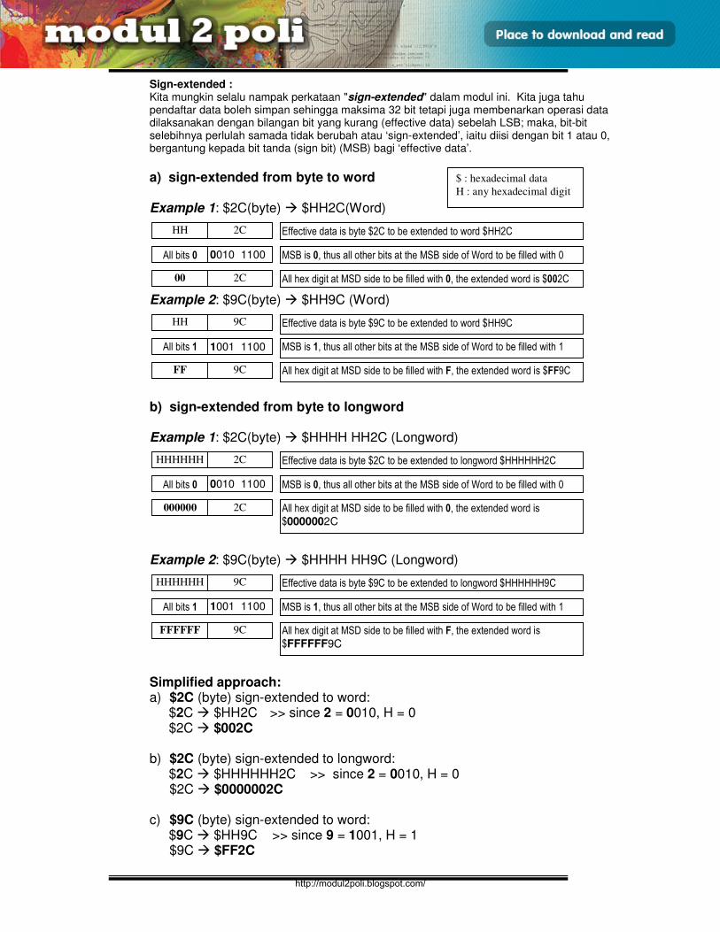
E3165 / UNIT 3 / 13
ASSEMBLY LANGUAGE
Sign-extended : Kita mungkin selalu nampak perkataan "sign-extended" dalam modul ini. Kita juga tahu pendaftar data boleh simpan sehingga maksima 32 bit tetapi juga membenarkan operasi data dilaksanakan dengan bilangan bit yang kurang (effective data) sebelah LSB; maka, bit-bit selebihnya perlulah samada tidak berubah atau ‘sign-extended’, iaitu diisi dengan bit 1 atau 0, bergantung kepada bit tanda (sign bit) (MSB) bagi ‘effective data’.
a) sign-extended from byte to word
Example 1: $2C(byte) $HH2C(Word) Example 2: $9C(byte) $HH9C (Word) b) sign-extended from byte to longword
Example 1: $2C(byte) $HHHH HH2C (Longword) Example 2: $9C(byte) $HHHH HH9C (Longword) Simplified approach: a) $2C (byte) sign-extended to word:
$2C $HH2C >> since 2 = 0010, H = 0 $2C $002C
b) $2C (byte) sign-extended to longword:
$2C $HHHHHH2C >> since 2 = 0010, H = 0 $2C $0000002C
c) $9C (byte) sign-extended to word:
$9C $HH9C >> since 9 = 1001, H = 1 $9C $FF2C
0010 1100 All bits 0
2C HH
2C 00
Effective data is byte $2C to be extended to word $HH2C
MSB is 0, thus all other bits at the MSB side of Word to be filled with 0
All hex digit at MSD side to be filled with 0, the extended word is $002C
1001 1100 All bits 1
9C HH
9C FF
Effective data is byte $9C to be extended to word $HH9C
MSB is 1, thus all other bits at the MSB side of Word to be filled with 1
All hex digit at MSD side to be filled with F, the extended word is $FF9C
0010 1100 All bits 0
2C HHHHHH
2C 000000
Effective data is byte $2C to be extended to longword $HHHHHH2C
MSB is 0, thus all other bits at the MSB side of Word to be filled with 0
All hex digit at MSD side to be filled with 0, the extended word is $0000002C
$ : hexadecimal data
H : any hexadecimal digit
1001 1100 All bits 1
9C HHHHHH
9C FFFFFF
Effective data is byte $9C to be extended to longword $HHHHHH9C
MSB is 1, thus all other bits at the MSB side of Word to be filled with 1
All hex digit at MSD side to be filled with F, the extended word is $FFFFFF9C
http://modul2poli.blogspot.com/
E3165 / UNIT 3 / 14
ASSEMBLY LANGUAGE
d) $9C (byte) sign-extended to longword:
$9C $HHHHHH9C >> since 9 = 1001, H = 1 $9C $FFFFFF2C
e) $912C (word) sign-extended to longword:
$912C $HHHH912C >> since 9 = 1001, H = 1 $912C $FFFF912C
Rujuk Pg : 5-3 Mod Mutlak Pendek
http://modul2poli.blogspot.com/
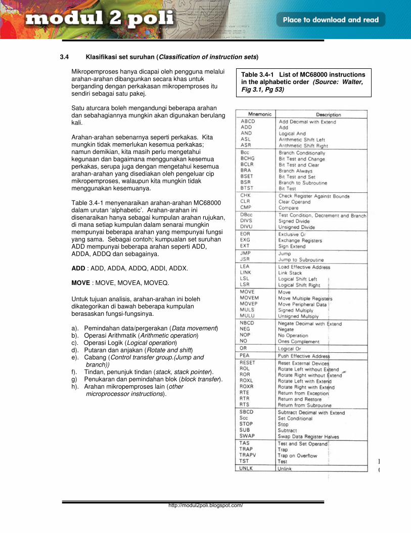
E3165 / UNIT 3 / 15
ASSEMBLY LANGUAGE
3.4 Klasifikasi set suruhan (Classification of instruction sets)
Mikropemproses hanya dicapai oleh pengguna melalui arahan-arahan dibangunkan secara khas untuk berganding dengan perkakasan mikropemproses itu sendiri sebagai satu pakej. Satu aturcara boleh mengandungi beberapa arahan dan sebahagiannya mungkin akan digunakan berulang kali. Arahan-arahan sebenarnya seperti perkakas. Kita mungkin tidak memerlukan kesemua perkakas; namun demikian, kita masih perlu mengetahui kegunaan dan bagaimana menggunakan kesemua perkakas, serupa juga dengan mengetahui kesemua arahan-arahan yang disediakan oleh pengeluar cip mikropemproses, walaupun kita mungkin tidak menggunakan kesemuanya. Table 3.4-1 menyenaraikan arahan-arahan MC68000 dalam urutan ‘alphabetic’. Arahan-arahan ini disenaraikan hanya sebagai kumpulan arahan rujukan, di mana setiap kumpulan dalam senarai mungkin mempunyai beberapa arahan yang mempunyai fungsi yang sama. Sebagai contoh; kumpualan set suruhan ADD mempunyai beberapa arahan seperti ADD, ADDA, ADDQ dan sebagainya. ADD : ADD, ADDA, ADDQ, ADDI, ADDX. MOVE : MOVE, MOVEA, MOVEQ.
Untuk tujuan analisis, arahan-arahan ini boleh dikategorikan di bawah beberapa kumpulan berasaskan fungsi-fungsinya. a). Pemindahan data/pergerakan (Data movement) b). Operasi Arithmatik (Arithmetic operation) c). Operasi Logik (Logical operation) d). Putaran dan anjakan (Rotate and shift) e). Cabang (Control transfer group.(Jump and
branch)) f). Tindan, penunjuk tindan (stack, stack pointer). g) Penukaran dan pemindahan blok (block transfer). h). Arahan mikropemproses lain (other
microprocessor instructions).
Table 3.4-1 List of MC68000 instructions in the alphabetic order (Source: Walter,
Fig 3.1, Pg 53)
http://modul2poli.blogspot.com/
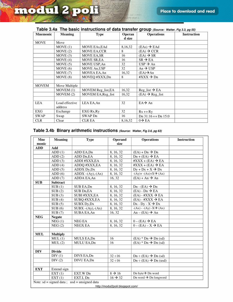
E3165 / UNIT 3 / 16
ASSEMBLY LANGUAGE
Table 3.4a The basic instructions of data transfer group (Source: Walter, Fig 3.3, pg 55)
Mnemonic Meaning Type Operan
d size
Operations Instruction
MOVE Move
MOVE (1) MOVE EAs,EAd 8,16,32 (EAs) EAd
MOVE (2) MOVE EA,CCR 8 (EA) CCR
MOVE (3) MOVE EA,SR 16 (EA) SR
MOVE (4) MOVE SR,EA 16 SR EA
MOVE (5) MOVE USP,An 32 USP An
MOVE (6) MOVE An,USP 32 An USP
MOVE (7) MOVEA EA,An 16,32 (EA)An
MOVE (8) MOVEQ #XXX,Dn 8 #XXX Dn
MOVEM Move Multiple
MOVEM (1) MOVEM Reg_list,EA 16,32 Reg_list EA
MOVEM (2) MOVEM EA,Reg_list 16,32 (EA) Reg_list
LEA Load effective
address
LEA EA,An 32 EA An
EXG Exchange EXG Rx,Ry 32 Rx ↔ Ry
SWAP Swap SWAP Dn 16 Dn 31:16 ↔ Dn 15:0
CLR Clear CLR EA 8,16,32 0 EA
Table 3.4b Binary arithmetic instructions (Source: Walter, Fig 3.6, pg 63)
Mne
monic
Meaning Type Operand
size
Operations Instruction
ADD Add
ADD (1) ADD EA,Dn 8, 16, 32 (EA) + Dn Dn
ADD (2) ADD Dn,EA 8, 16, 32 Dn + (EA) EA
ADD (3) ADDI #XXX,EA 8, 16, 32 #XXX + (EA) EA
ADD (4) ADDQ #XXX,EA 8, 16, 32 #XXX + (EA) EA
ADD (5) ADDX Dy,Dx 8, 16, 32 Dy + Dx + X Dx
ADD (6) ADDX –(Ay),-(Ax) 8, 16, 32 -(Ay)+ -(Ax)+X (Ax)
ADD (7) ADDA EA,An 16, 32 (EA) + An An
SUB Subtract
SUB (1) SUB EA,Dn 8, 16, 32 Dn - (EA) Dn
SUB (2) SUB Dn,EA 8, 16, 32 (EA) - Dn EA
SUB (3) SUBI #XXX,EA 8, 16, 32 (EA) - #XXX EA
SUB (4) SUBQ #XXX,EA 8, 16, 32 (EA) - #XXX EA
SUB (5) SUBX Dy,Dx 8, 16, 32 Dx - Dy - X Dx
SUB (6) SUBX –(Ay),-(Ax) 8, 16, 32 -(Ax) - -(Ay) -X (Ax)
SUB (7) SUBA EA,An 16, 32 An – (EA) An
NEG Negate
NEG (1) NEG EA 8, 16, 32 0 – (EA) EA
NEG (2) NEGX EA 8, 16, 32 0 – (EA) – X EA
MUL Multiply
MUL (1) MULS EA,Dn 16 (EA) * Dn Dn (sd)
MUL (2) MULU EA,Dn 16 (EA) * Dn Dn (sd)
DIV Divide
DIV (1) DIVS EA,Dn 32 ÷16 Dn ÷ (EA) Dn (sd)
DIV (2) DIVU EA,Dn 32 ÷16 Dn ÷ (EA) Dn (usd)
EXT Extend sign
EXT (1) EXT.W Dn 8 16 Dn byte Dn word
EXT (1) EXT.L Dn 16 32 Dn word Dn longword
Note: sd = signed data ; usd = unsigned data
http://modul2poli.blogspot.com/
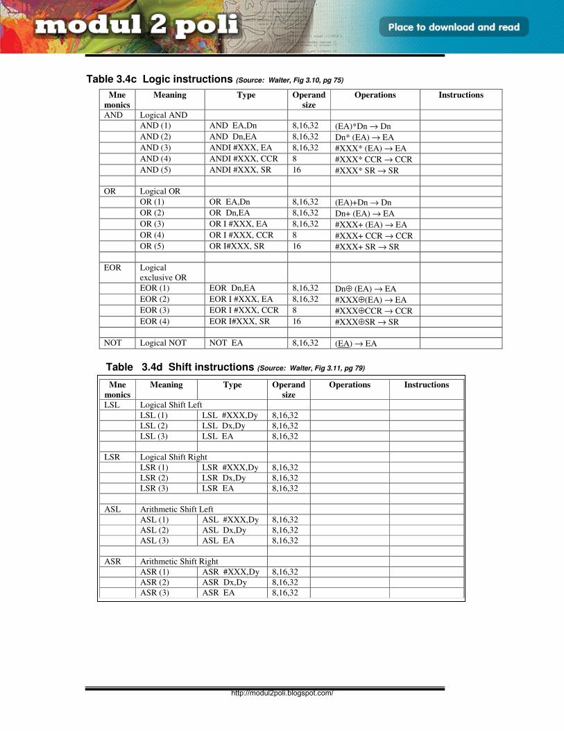
E3165 / UNIT 3 / 17
ASSEMBLY LANGUAGE
Table 3.4c Logic instructions (Source: Walter, Fig 3.10, pg 75)
Table 3.4d Shift instructions (Source: Walter, Fig 3.11, pg 79)
Mne
monics
Meaning Type Operand
size
Operations Instructions
AND Logical AND
AND (1) AND EA,Dn 8,16,32 (EA)*Dn → Dn
AND (2) AND Dn,EA 8,16,32 Dn* (EA) → EA
AND (3) ANDI #XXX, EA 8,16,32 #XXX* (EA) → EA
AND (4) ANDI #XXX, CCR 8 #XXX* CCR → CCR
AND (5) ANDI #XXX, SR 16 #XXX* SR → SR
OR Logical OR
OR (1) OR EA,Dn 8,16,32 (EA)+Dn → Dn
OR (2) OR Dn,EA 8,16,32 Dn+ (EA) → EA
OR (3) OR I #XXX, EA 8,16,32 #XXX+ (EA) → EA
OR (4) OR I #XXX, CCR 8 #XXX+ CCR → CCR
OR (5) OR I#XXX, SR 16 #XXX+ SR → SR
EOR Logical
exclusive OR
EOR (1) EOR Dn,EA 8,16,32 Dn⊕ (EA) → EA
EOR (2) EOR I #XXX, EA 8,16,32 #XXX⊕(EA) → EA
EOR (3) EOR I #XXX, CCR 8 #XXX⊕CCR → CCR
EOR (4) EOR I#XXX, SR 16 #XXX⊕SR → SR
NOT Logical NOT NOT EA 8,16,32 (EA) → EA
Mne
monics
Meaning Type Operand
size
Operations Instructions
LSL Logical Shift Left
LSL (1) LSL #XXX,Dy 8,16,32
LSL (2) LSL Dx,Dy 8,16,32
LSL (3) LSL EA 8,16,32
LSR Logical Shift Right
LSR (1) LSR #XXX,Dy 8,16,32
LSR (2) LSR Dx,Dy 8,16,32
LSR (3) LSR EA 8,16,32
ASL Arithmetic Shift Left
ASL (1) ASL #XXX,Dy 8,16,32
ASL (2) ASL Dx,Dy 8,16,32
ASL (3) ASL EA 8,16,32
ASR Arithmetic Shift Right
ASR (1) ASR #XXX,Dy 8,16,32
ASR (2) ASR Dx,Dy 8,16,32
ASR (3) ASR EA 8,16,32
http://modul2poli.blogspot.com/
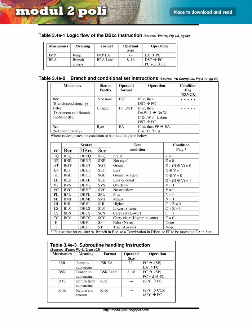
E3165 / UNIT 3 / 18
ASSEMBLY LANGUAGE
Table 3.4e-1 Logic flow of the DBcc instruction (Source: Walter, Fig 4.5, pg 96)
Table 3.4e-2 Branch and conditional set instructions (Source: Yu-Cheng Liu, Fig 3-11, pg 57)
Mnemonics Meaning Format Operand
Size
Operation
JMP Jump JMP EA - - EA PC
BRA Branch
always
BRA Label 8, 16 DST PC
PC + d PC
Mnemonic Size or
Postfix
Operand
format
Operation Condition
flag
NZVCX
Bcc
(Branch conditionally)
.S or none DST If cc, then
DST PC - - - - -
DBcc
(Decrement and Branch
conditionally)
Unsized Dn, DST If cc, then
Dn.W -1 Dn.W
If Dn.W ≠ -1, then
DST PC
- - - - -
Scc
(Set conditionally)
Byte EA If cc, then FF EA
Else 00 EA - - - - -
Where cc designates the condition to be tested as given below.
cc Syntax Test
condition
Condition
Flag * Bcc DBcc Scc EQ BEQ DBEQ SEQ Equal Z = 1
NE BNE DBNE SNE Not equal Z = 0
GT BGT DBGT SGT Greater Z + (N ⊕ V) = 0
LT BLT DBLT SLT Less N ⊕ V = 1
GE BGE DBGE SGE Greater or equal N ⊕ V = 0
LE BLE DBLE SLE Less or equal Z + (N ⊕ V) = 1
VS BVS DBVS SVS Overflow V = 1
VC BVC DBVC SVC No overflow V = 0
PL BPL DBPL SPL Plus N = 0
MI BMI DBMI SMI Minus N = 1
HI BHI DBHI SHI Higher C + Z = 0
LS BLS DBLS SLS Lower or same C + Z = 1
CS BCS DBCS SCS Carry set (Lower) C = 1
CC BCC DBCC SCC Carry clear (Higher or same) C = 0
F DBF SF False (Never) None
T DBT ST True (Always) None
* Flag setting for causing :a Branch in Bcc, or a Termination in DBcc, or FF to be moved to EA in Scc.
Table 3.4e-3 Subroutine handling instruction (Source: Walter, Fig 4.10, pg 103)
Mnemonics Meaning Format Operand
Size
Operation
JSR Jump to
subroutine
JSR EA 32- PC -(SP)
EA PC
BSR Branch to
subroutine
BSR Label 8, 16 PC -(SP)
PC + d PC
RTS Return from
subroutine
RTS --- (SP)+ PC
RTR Return and
restore
RTR --- (SP)+ CCR
(SP)+ PC
http://modul2poli.blogspot.com/
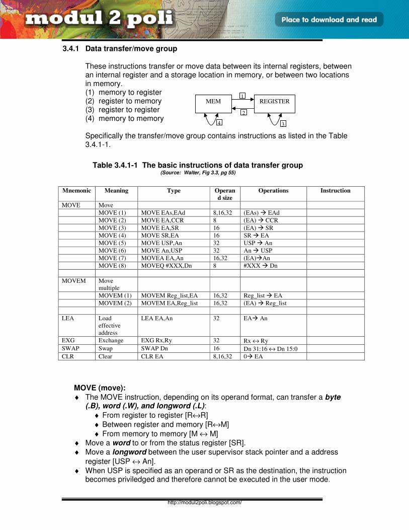
E3165 / UNIT 3 / 19
ASSEMBLY LANGUAGE
3.4.1 Data transfer/move group These instructions transfer or move data between its internal registers, between an internal register and a storage location in memory, or between two locations in memory. (1) memory to register (2) register to memory (3) register to register (4) memory to memory Specifically the transfer/move group contains instructions as listed in the Table 3.4.1-1.
MOVE (move):
♦ The MOVE instruction, depending on its operand format, can transfer a byte (.B), word (.W), and longword (.L):
♦ From register to register [R↔R]
♦ Between register and memory [R↔M]
♦ From memory to memory [M ↔ M]
♦ Move a word to or from the status register [SR].
♦ Move a longword between the user supervisor stack pointer and a address
register [USP ↔ An].
♦ When USP is specified as an operand or SR as the destination, the instruction becomes priviledged and therefore cannot be executed in the user mode.
MEM REGISTER
Table 3.4.1-1 The basic instructions of data transfer group (Source: Walter, Fig 3.3, pg 55)
1
2
3 4
Mnemonic Meaning Type Operan
d size
Operations Instruction
MOVE Move
MOVE (1) MOVE EAs,EAd 8,16,32 (EAs) EAd
MOVE (2) MOVE EA,CCR 8 (EA) CCR
MOVE (3) MOVE EA,SR 16 (EA) SR
MOVE (4) MOVE SR,EA 16 SR EA
MOVE (5) MOVE USP,An 32 USP An
MOVE (6) MOVE An,USP 32 An USP
MOVE (7) MOVEA EA,An 16,32 (EA)An
MOVE (8) MOVEQ #XXX,Dn 8 #XXX Dn
MOVEM Move
multiple
MOVEM (1) MOVEM Reg_list,EA 16,32 Reg_list EA
MOVEM (2) MOVEM EA,Reg_list 16,32 (EA) Reg_list
LEA Load
effective
address
LEA EA,An 32 EA An
EXG Exchange EXG Rx,Ry 32 Rx ↔ Ry
SWAP Swap SWAP Dn 16 Dn 31:16 ↔ Dn 15:0
CLR Clear CLR EA 8,16,32 0 EA
http://modul2poli.blogspot.com/

E3165 / UNIT 3 / 20
ASSEMBLY LANGUAGE
Notes: When data is moved from one register to another register, the data in the source register is remained. The operation is actually copy the data in the source register to the destination register. Rujuk Pg: 5-4 MOVE.s punca, Destinasi
http://modul2poli.blogspot.com/
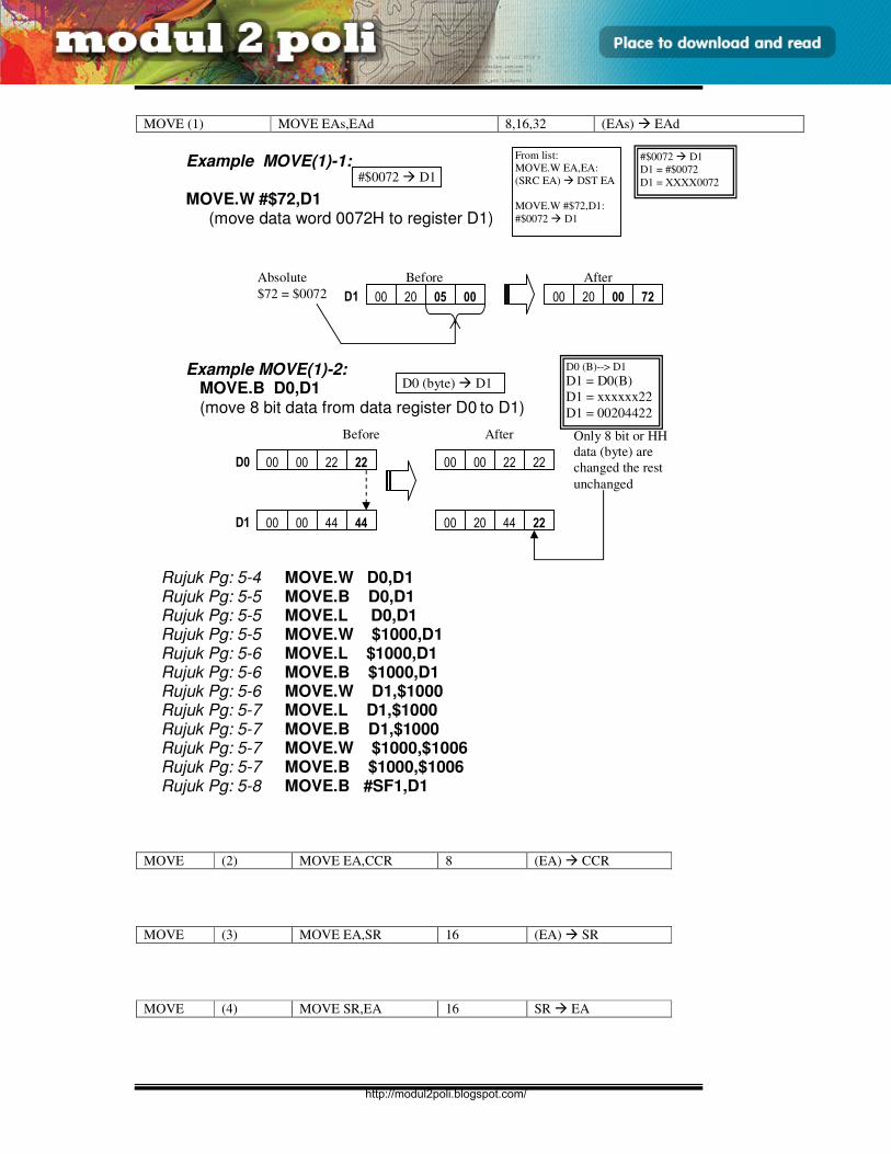
E3165 / UNIT 3 / 21
ASSEMBLY LANGUAGE
MOVE (1) MOVE EAs,EAd 8,16,32 (EAs) EAd
Example MOVE(1)-1: MOVE.W #$72,D1 (move data word 0072H to register D1)
Example MOVE(1)-2: MOVE.B D0,D1 (move 8 bit data from data register D0 to D1)
Rujuk Pg: 5-4 MOVE.W D0,D1 Rujuk Pg: 5-5 MOVE.B D0,D1 Rujuk Pg: 5-5 MOVE.L D0,D1 Rujuk Pg: 5-5 MOVE.W $1000,D1 Rujuk Pg: 5-6 MOVE.L $1000,D1 Rujuk Pg: 5-6 MOVE.B $1000,D1 Rujuk Pg: 5-6 MOVE.W D1,$1000 Rujuk Pg: 5-7 MOVE.L D1,$1000 Rujuk Pg: 5-7 MOVE.B D1,$1000 Rujuk Pg: 5-7 MOVE.W $1000,$1006 Rujuk Pg: 5-7 MOVE.B $1000,$1006 Rujuk Pg: 5-8 MOVE.B #SF1,D1
MOVE (2) MOVE EA,CCR 8 (EA) CCR
MOVE (3) MOVE EA,SR 16 (EA) SR
MOVE (4) MOVE SR,EA 16 SR EA
D0 (byte) D1
From list:
MOVE.W EA,EA:
(SRC EA) DST EA
MOVE.W #$72,D1:
#$0072 D1
#$0072 D1
Before After Absolute
$72 = $0072 00 20 05 00 D1 00 20 00 72
Only 8 bit or HH
data (byte) are
changed the rest
unchanged
Before After
00 00 22 22 D0 00 00 22 22
00 00 44 44 D1 00 20 44 22
#$0072 D1
D1 = #$0072
D1 = XXXX0072
D0 (B)--> D1
D1 = D0(B)
D1 = xxxxxx22
D1 = 00204422
http://modul2poli.blogspot.com/
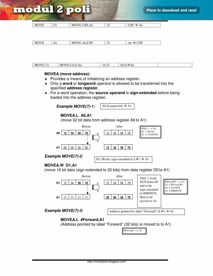
E3165 / UNIT 3 / 22
ASSEMBLY LANGUAGE
MOVE (5) MOVE USP,An 32 USP An
MOVE (6) MOVE An,USP 32 An USP
MOVE (7) MOVEA EA,An 16,32 (EA)An
MOVEA (move address):
♦ Provides a means of initializing an address register.
♦ Only a word or longword operand is allowed to be transferred into the specified address register.
♦ For a word operation, the source operand is sign-extended before being loaded into the address register.
Example MOVE(7)-1:
MOVEA.L A0,A1 (move 32 bit data from address register A0 to A1)
Example MOVE(7)-2: MOVEA.W D1,A1 (move 16 bit data (sign-extended to 32 bits) from data register D0 to A1)
Example MOVE(7)-3:
MOVEA.L #Forward,A1 (Address pointed by label “Forward” (32 bits) is moved to to A1)
A0 (Longword) A1
Before After
12 34 56 78 A0 12 34 56 78
00 00 00 00 A1 12 34 56 78
D1 (Word, sign-extended to LW) A1
Before After
12 34 56 78 D1 12 34 56 78
11 11 11 11 A1 00 00 56 78
Only 1 word
5678 from D1
and to be
sign-extended
to 00005678,
then to be
moved to A1
Address pointed by label “Forward” (LW) A1
A0(L) --> A1
A1 = A0 (L)
A1 = 12345678
D0(ssssW) --> A1 A1 = D0 (ssssW)
A1 = ssss5678
A1 = 00005678
#Forward --> A1
http://modul2poli.blogspot.com/
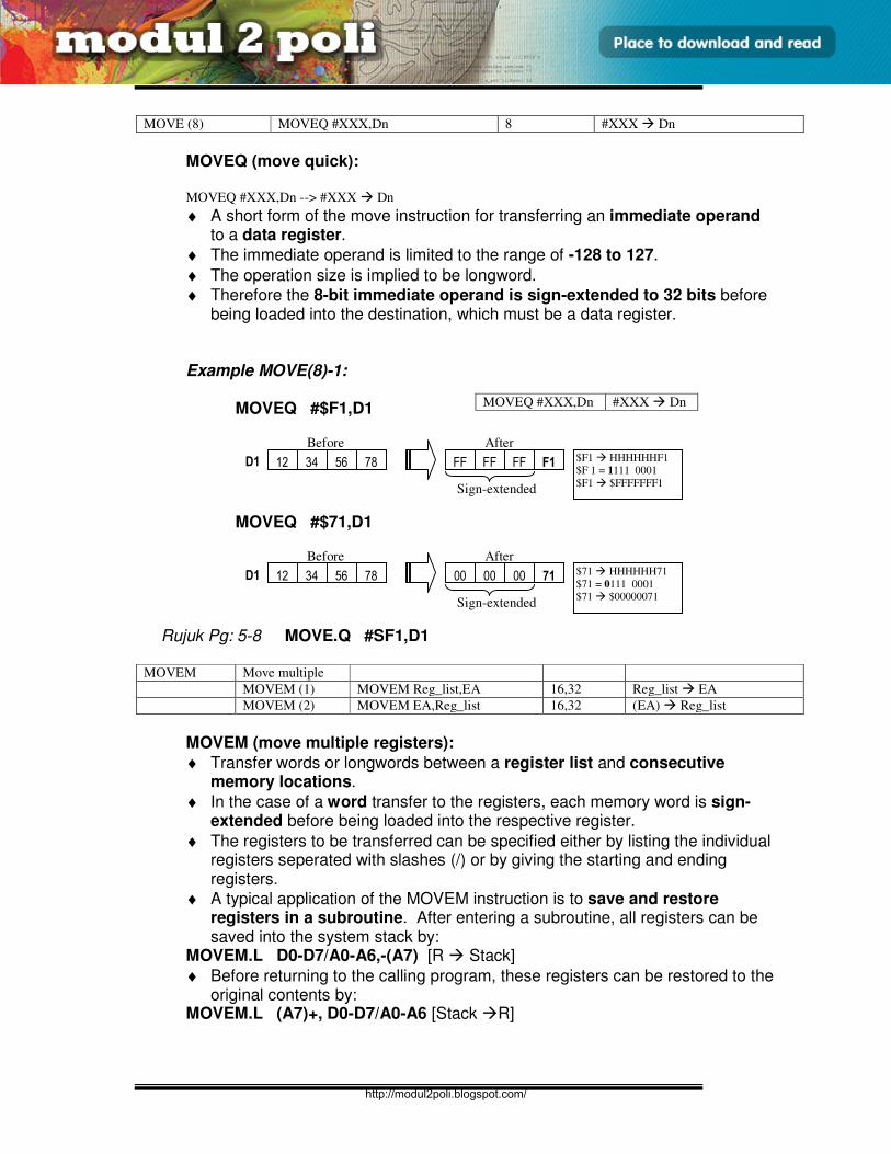
E3165 / UNIT 3 / 23
ASSEMBLY LANGUAGE
MOVE (8) MOVEQ #XXX,Dn 8 #XXX Dn
MOVEQ (move quick): MOVEQ #XXX,Dn --> #XXX Dn ♦ A short form of the move instruction for transferring an immediate operand
to a data register.
♦ The immediate operand is limited to the range of -128 to 127.
♦ The operation size is implied to be longword.
♦ Therefore the 8-bit immediate operand is sign-extended to 32 bits before being loaded into the destination, which must be a data register.
Example MOVE(8)-1: MOVEQ #$F1,D1
MOVEQ #$71,D1
Rujuk Pg: 5-8 MOVE.Q #SF1,D1
MOVEM Move multiple
MOVEM (1) MOVEM Reg_list,EA 16,32 Reg_list EA
MOVEM (2) MOVEM EA,Reg_list 16,32 (EA) Reg_list
MOVEM (move multiple registers):
♦ Transfer words or longwords between a register list and consecutive memory locations.
♦ In the case of a word transfer to the registers, each memory word is sign-extended before being loaded into the respective register.
♦ The registers to be transferred can be specified either by listing the individual registers seperated with slashes (/) or by giving the starting and ending registers.
♦ A typical application of the MOVEM instruction is to save and restore registers in a subroutine. After entering a subroutine, all registers can be saved into the system stack by:
MOVEM.L D0-D7/A0-A6,-(A7) [R Stack]
♦ Before returning to the calling program, these registers can be restored to the original contents by:
MOVEM.L (A7)+, D0-D7/A0-A6 [Stack R]
$F1 HHHHHHF1
$F 1 = 1111 0001
$F1 $FFFFFFF1
Before After
12 34 56 78 D1 FF FF FF F1
Sign-extended
$71 HHHHHH71
$71 = 0111 0001
$71 $00000071
Before After
12 34 56 78 D1 00 00 00 71
Sign-extended
MOVEQ #XXX,Dn #XXX Dn
http://modul2poli.blogspot.com/

E3165 / UNIT 3 / 24
ASSEMBLY LANGUAGE
♦ In the memory, the content of selected registers are always stored in such a way that D0 corresponds to the lowest address, D1 to the next, …., followed by A0 to A7, with A7 corresponds to the highest memory address.
♦ In other words, irrespective the sequence of the registers numbering stated in the instruction, the data transfering process will be rearranged from lowest to highest sequence.
♦ Figure 3.4.1-1 shows the comparison of the four MOVEM instructions.
http://modul2poli.blogspot.com/
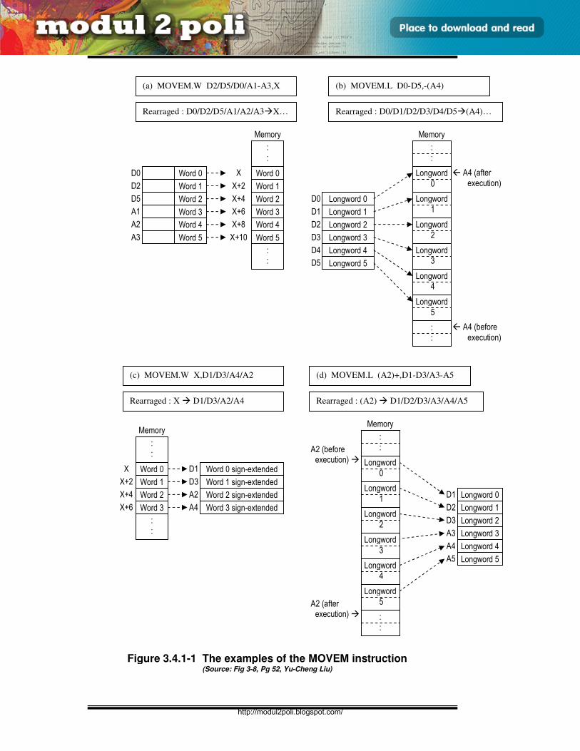
E3165 / UNIT 3 / 25
ASSEMBLY LANGUAGE
Figure 3.4.1-1 The examples of the MOVEM instruction (Source: Fig 3-8, Pg 52, Yu-Cheng Liu)
Word 0 D0
(a) MOVEM.W D2/D5/D0/A1-A3,X
Word 1 D2
Word 2 D5
Word 3 A1
Word 4 A2
Word 5 A3
Word 0 X
Word 1 X+2
Word 2 X+4
Word 3 X+6
Word 4 X+8
Word 5 X+10
: :
Memory
: :
Rearraged : D0/D2/D5/A1/A2/A3X…
Longword 0 D0
(b) MOVEM.L D0-D5,-(A4)
Longword 1 D1
Longword 2 D2
Longword 3 D3
Longword 4 D4
Longword 5 D5
Memory
Rearraged : D0/D1/D2/D3/D4/D5(A4)…
Longword 1
Longword 2
Longword 0
Longword 3
Longword 4
Longword 5
: :
: :
A4 (after execution)
A4 (before execution)
(c) MOVEM.W X,D1/D3/A4/A2
Rearraged : X D1/D3/A2/A4
Word 0 D1
Word 1 D3
Word 2 A2
Word 3 A4
Word 0 sign-extended X
Word 1 sign-extended X+2
Word 2 sign-extended X+4
Word 3 sign-extended X+6
: :
Memory
: :
Longword 0 D1
(d) MOVEM.L (A2)+,D1-D3/A3-A5
Longword 1 D2
Longword 2 D3
Longword 3 A3
Longword 4 A4
Longword 5 A5
Memory
Rearraged : (A2) D1/D2/D3/A3/A4/A5
Longword 1
Longword 2
Longword 0
Longword 3
Longword 4
Longword 5
: :
: :
A2 (after execution)
A2 (before execution)
http://modul2poli.blogspot.com/
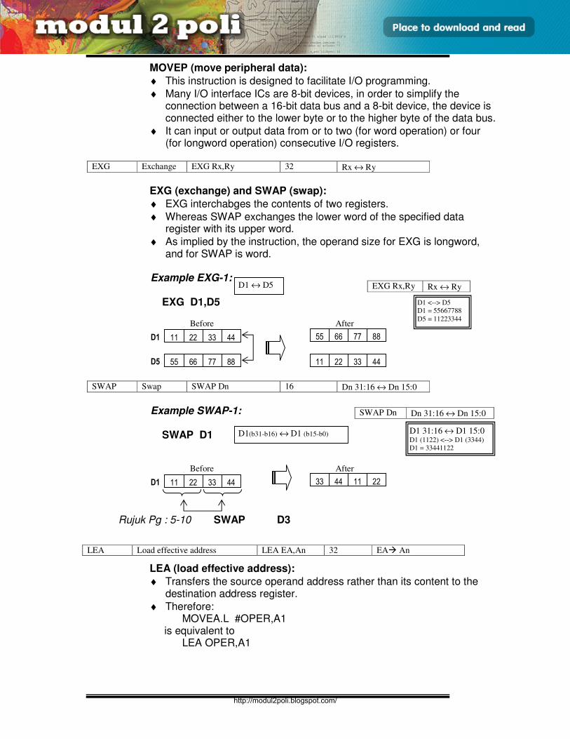
E3165 / UNIT 3 / 26
ASSEMBLY LANGUAGE
MOVEP (move peripheral data):
♦ This instruction is designed to facilitate I/O programming.
♦ Many I/O interface ICs are 8-bit devices, in order to simplify the connection between a 16-bit data bus and a 8-bit device, the device is connected either to the lower byte or to the higher byte of the data bus.
♦ It can input or output data from or to two (for word operation) or four (for longword operation) consecutive I/O registers.
EXG Exchange EXG Rx,Ry 32 Rx ↔ Ry
EXG (exchange) and SWAP (swap):
♦ EXG interchabges the contents of two registers.
♦ Whereas SWAP exchanges the lower word of the specified data register with its upper word.
♦ As implied by the instruction, the operand size for EXG is longword, and for SWAP is word.
Example EXG-1:
EXG D1,D5
SWAP Swap SWAP Dn 16 Dn 31:16 ↔ Dn 15:0
Example SWAP-1:
SWAP D1
Rujuk Pg : 5-10 SWAP D3
LEA (load effective address):
♦ Transfers the source operand address rather than its content to the destination address register.
♦ Therefore: MOVEA.L #OPER,A1
is equivalent to LEA OPER,A1
LEA Load effective address LEA EA,An 32 EA An
D1 ↔ D5
Before After
11 22 33 44 D1
55 66 77 88 D5 11 22 33 44
55 66 77 88
D1(b31-b16) ↔ D1 (b15-b0)
Before After
11 22 33 44 D1 33 44 11 22
D1 31:16 ↔ D1 15:0 D1 (1122) <--> D1 (3344)
D1 = 33441122
D5 = 11223344
SWAP Dn Dn 31:16 ↔ Dn 15:0
D1 <--> D5
D1 = 55667788
D5 = 11223344
EXG Rx,Ry Rx ↔ Ry
http://modul2poli.blogspot.com/
E3165 / UNIT 3 / 27
ASSEMBLY LANGUAGE
CLR Clear CLR EA 8,16,32 0 EA
Rujuk Pg : 5-1 CLR.s Destination Rujuk Pg : 5-1 CLR.W D1 Rujuk Pg : 5-1 CLR.B D2 Rujuk Pg : 5-1 CLR.L D7 Rujuk Pg : 5-2 CLR.B $10000 Rujuk Pg : 5-2 CLR.W $10000 Rujuk Pg : 5-2 CLR.L $10000 Rujuk Pg : 5-3 CLR.B $1000
http://modul2poli.blogspot.com/

E3165 / UNIT 3 / 28
ASSEMBLY LANGUAGE
3.4.2 Arithmetic Operation
♦ Similarly as the operation of mathematic, addition (+), subtraction (-), multiplication (x), division (÷)
♦ Binary arithmetic instructions performs signed and unsigned operations.
♦ Table 3.4.2-1 shows the detailed elements of binary arithmetic instructions.
Table 3.4.2-1 Binary arithmetic instructions (Source: Walter, Fig 3.6, pg 63)
Mne
monic
Meaning Type Operand
size
Operations Instruction
ADD Add
ADD (1) ADD EA,Dn 8, 16, 32 (EA) + Dn Dn
ADD (2) ADD Dn,EA 8, 16, 32 Dn + (EA) EA
ADD (3) ADDI #XXX,EA 8, 16, 32 #XXX + (EA) EA
ADD (4) ADDQ #XXX,EA 8, 16, 32 #XXX + (EA) EA
ADD (5) ADDX Dy,Dx 8, 16, 32 Dy + Dx + X Dx
ADD (6) ADDX –(Ay),-(Ax) 8, 16, 32 -(Ay)+ -(Ax)+X (Ax)
ADD (7) ADDA EA,An 16, 32 (EA) + An An
SUB Subtract
SUB (1) SUB EA,Dn 8, 16, 32 Dn - (EA) Dn
SUB (2) SUB Dn,EA 8, 16, 32 (EA) - Dn EA
SUB (3) SUBI #XXX,EA 8, 16, 32 (EA) - #XXX EA
SUB (4) SUBQ #XXX,EA 8, 16, 32 (EA) - #XXX EA
SUB (5) SUBX Dy,Dx 8, 16, 32 Dx - Dy - X Dx
SUB (6) SUBX –(Ay),-(Ax) 8, 16, 32 -(Ax) - -(Ay) -X (Ax)
SUB (7) SUBA EA,An 16, 32 An – (EA) An
NEG Negate
NEG (1) NEG EA 8, 16, 32 0 – (EA) EA
NEG (2) NEGX EA 8, 16, 32 0 – (EA) – X EA
MUL Multiply
MUL (1) MULS EA,Dn 16 (EA) * Dn Dn (sd)
MUL (2) MULU EA,Dn 16 (EA) * Dn Dn (sd)
DIV Divide
DIV (1) DIVS EA,Dn 32 ÷16 Dn ÷ (EA) Dn (sd)
DIV (2) DIVU EA,Dn 32 ÷16 Dn ÷ (EA) Dn (usd)
EXT Extend
sign
EXT (1) EXT.W Dn 8 16 Dn byte Dn word
EXT (1) EXT.L Dn 16 32 Dn word Dn longword
Note: sd = signed data ; usd = unsigned data
http://modul2poli.blogspot.com/
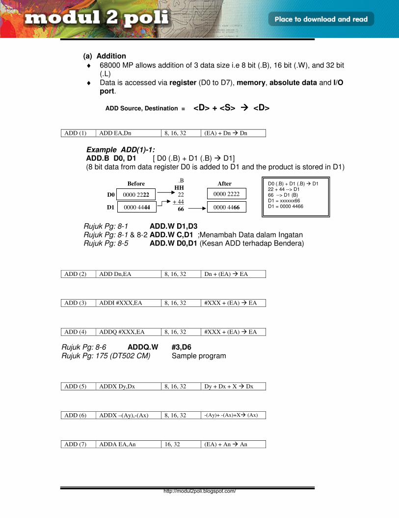
E3165 / UNIT 3 / 29
ASSEMBLY LANGUAGE
(a) Addition
♦ 68000 MP allows addition of 3 data size i.e 8 bit (.B), 16 bit (.W), and 32 bit (.L)
♦ Data is accessed via register (D0 to D7), memory, absolute data and I/O port.
ADD Source, Destination = <D> + <S> <D>
ADD (1) ADD EA,Dn 8, 16, 32 (EA) + Dn Dn
Example ADD(1)-1: ADD.B D0, D1 [ D0 (.B) + D1 (.B) D1] (8 bit data from data register D0 is added to D1 and the product is stored in D1)
Rujuk Pg: 8-1 ADD.W D1,D3 Rujuk Pg: 8-1 & 8-2 ADD.W C,D1 ;Menambah Data dalam Ingatan Rujuk Pg: 8-5 ADD.W D0,D1 (Kesan ADD terhadap Bendera)
ADD (2) ADD Dn,EA 8, 16, 32 Dn + (EA) EA
ADD (3) ADDI #XXX,EA 8, 16, 32 #XXX + (EA) EA
ADD (4) ADDQ #XXX,EA 8, 16, 32 #XXX + (EA) EA
Rujuk Pg: 8-6 ADDQ.W #3,D6 Rujuk Pg: 175 (DT502 CM) Sample program
ADD (5) ADDX Dy,Dx 8, 16, 32 Dy + Dx + X Dx
ADD (6) ADDX –(Ay),-(Ax) 8, 16, 32 -(Ay)+ -(Ax)+X (Ax)
ADD (7) ADDA EA,An 16, 32 (EA) + An An
0000 2222
Before
D0
0000 4444 D1
.B
HH 22
+ 44
66
0000 2222
After
0000 4466
D0 (.B) + D1 (.B) D1 22 + 44 --> D1 66 --> D1 (B) D1 = xxxxxx66 D1 = 0000 4466
http://modul2poli.blogspot.com/
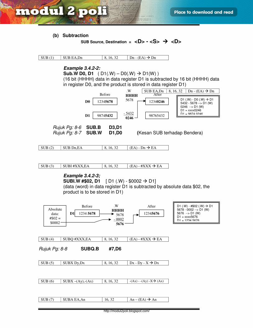
E3165 / UNIT 3 / 30
ASSEMBLY LANGUAGE
(b) Subtraction
SUB Source, Destination = <D> - <S> <D>
SUB (1) SUB EA,Dn 8, 16, 32 Dn - (EA) Dn
Example 3.4.2-2: Sub.W D0, D1 ( D1(.W) – D0(.W) D1(W) ) (16 bit (HHHH) data in data register D1 is subtracted by 16 bit (HHHH) data in register D0, and the product is stored in data register D1)
Rujuk Pg: 8-6 SUB.B D3,D1 Rujuk Pg: 8-7 SUB.W D1,D0 (Kesan SUB terhadap Bendera)
SUB (2) SUB Dn,EA 8, 16, 32 (EA) - Dn EA
SUB (3) SUBI #XXX,EA 8, 16, 32 (EA) - #XXX EA
Example 3.4.2-3; SUBI.W #$02, D1 [ D1 (.W) - $0002 D1] (data (word) in data register D1 is subtracted by absolute data $02, the product is to be stored in D1)
SUB (4) SUBQ #XXX,EA 8, 16, 32 (EA) - #XXX EA
Rujuk Pg: 8-8 SUBQ.B #7,D6
SUB (5) SUBX Dy,Dx 8, 16, 32 Dx - Dy - X Dx
SUB (6) SUBX –(Ay),-(Ax) 8, 16, 32 -(Ax) - -(Ay) -X (Ax)
SUB (7) SUBA EA,An 16, 32 An – (EA) An
.W
HHHH
5678
- 0002
5676
1234 5678
Before
D1 12345676
After Absolute
data:
#$02 =
$0002
D0
D1
12345678
Before
98745432
.W
HHHH
5678
- 5432
0246
12340246
After
98765432
SUB EA,Dn 8, 16, 32 Dn - (EA) Dn
D1 (.W) - D0 (.W) D1 5432 - 5678 --> D1 (W) 0246 --> D1 (W) D1 = xxxx0246 D1 = 9874 0246
D1 (.W) - #$02 (.W) D1 5678 - 0002 --> D1 (W) 5676 --> D1 (W) D1 = xxxx5676 D1 = 1234 5676
http://modul2poli.blogspot.com/
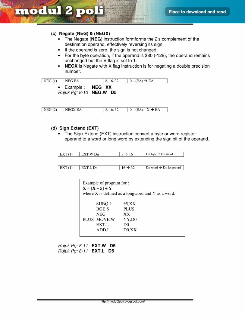
E3165 / UNIT 3 / 31
ASSEMBLY LANGUAGE
(c) Negate (NEG) & (NEGX)
• The Negate (NEG) instruction formforms the 2’s complement of the destination operand, effectively reversing its sign.
• If the operand is zero, the sign is not changed.
• For the byte operation, if the operand is $80 (-128), the operand remains unchanged but the V flag is set to 1.
• NEGX is Negate with X flag instruction is for negating a double precision number.
• Example : NEG XX Rujuk Pg: 8-10 NEG.W D5
(d) Sign Extend (EXT)
• The Sign-Extend (EXT) instruction convert a byte or word register operand to a word or long word by extending the sign bit of the operand.
EXT (1) EXT.W Dn 8 16 Dn byte Dn word
EXT (1) EXT.L Dn 16 32 Dn word Dn longword
Rujuk Pg: 8-11 EXT.W D5 Rujuk Pg: 8-11 EXT.L D5
NEG (1) NEG EA 8, 16, 32 0 – (EA) EA
NEG (2) NEGX EA 8, 16, 32 0 – (EA) – X EA
Example of program for :
X = [X – 5] + Y
where X is defined as a longword and Y as a word.
SUBQ.L #5,XX
BGE.S PLUS
NEG XX
PLUS MOVE.W YY,D0
EXT.L D0
ADD.L D0,XX
http://modul2poli.blogspot.com/
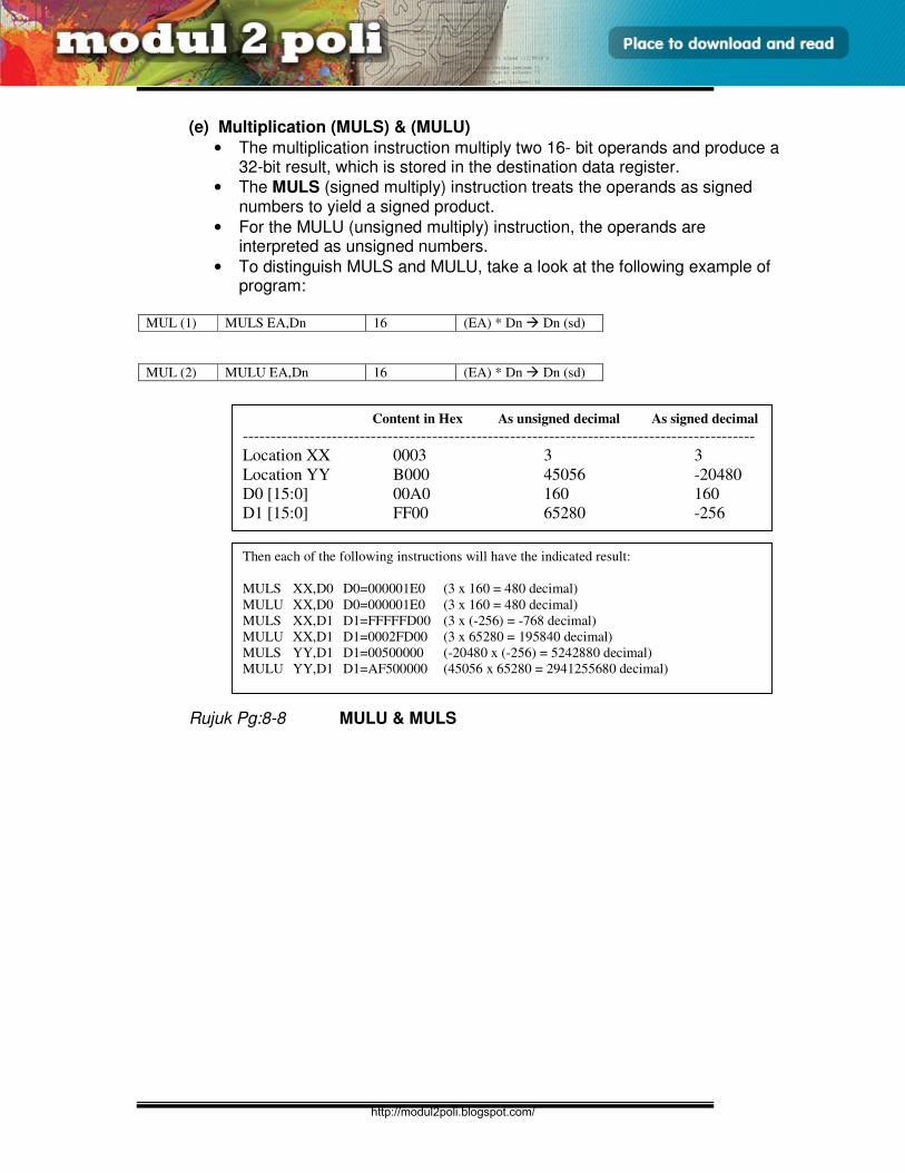
E3165 / UNIT 3 / 32
ASSEMBLY LANGUAGE
(e) Multiplication (MULS) & (MULU)
• The multiplication instruction multiply two 16- bit operands and produce a 32-bit result, which is stored in the destination data register.
• The MULS (signed multiply) instruction treats the operands as signed numbers to yield a signed product.
• For the MULU (unsigned multiply) instruction, the operands are interpreted as unsigned numbers.
• To distinguish MULS and MULU, take a look at the following example of program:
MUL (1) MULS EA,Dn 16 (EA) * Dn Dn (sd)
MUL (2) MULU EA,Dn 16 (EA) * Dn Dn (sd)
Rujuk Pg:8-8 MULU & MULS
Content in Hex As unsigned decimal As signed decimal
--------------------------------------------------------------------------------------------
Location XX 0003 3 3
Location YY B000 45056 -20480
D0 [15:0] 00A0 160 160
D1 [15:0] FF00 65280 -256
Then each of the following instructions will have the indicated result:
MULS XX,D0 D0=000001E0 (3 x 160 = 480 decimal)
MULU XX,D0 D0=000001E0 (3 x 160 = 480 decimal)
MULS XX,D1 D1=FFFFFD00 (3 x (-256) = -768 decimal)
MULU XX,D1 D1=0002FD00 (3 x 65280 = 195840 decimal)
MULS YY,D1 D1=00500000 (-20480 x (-256) = 5242880 decimal)
MULU YY,D1 D1=AF500000 (45056 x 65280 = 2941255680 decimal)
http://modul2poli.blogspot.com/
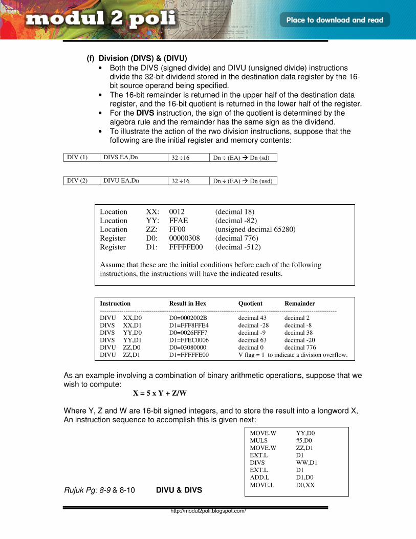
E3165 / UNIT 3 / 33
ASSEMBLY LANGUAGE
(f) Division (DIVS) & (DIVU)
• Both the DIVS (signed divide) and DIVU (unsigned divide) instructions divide the 32-bit dividend stored in the destination data register by the 16-bit source operand being specified.
• The 16-bit remainder is returned in the upper half of the destination data register, and the 16-bit quotient is returned in the lower half of the register.
• For the DIVS instruction, the sign of the quotient is determined by the algebra rule and the remainder has the same sign as the dividend.
• To illustrate the action of the rwo division instructions, suppose that the following are the initial register and memory contents:
DIV (1) DIVS EA,Dn 32 ÷16 Dn ÷ (EA) Dn (sd)
DIV (2) DIVU EA,Dn 32 ÷16 Dn ÷ (EA) Dn (usd)
As an example involving a combination of binary arithmetic operations, suppose that we wish to compute: X = 5 x Y + Z/W
Where Y, Z and W are 16-bit signed integers, and to store the result into a longword X, An instruction sequence to accomplish this is given next: Rujuk Pg: 8-9 & 8-10 DIVU & DIVS
Instruction Result in Hex Quotient Remainder
---------------------------------------------------------------------------------------------------------------
DIVU XX,D0 D0=0002002B decimal 43 decimal 2
DIVS XX,D1 D1=FFF8FFE4 decimal -28 decimal -8
DIVS YY,D0 D0=0026FFF7 decimal -9 decimal 38
DIVS YY,D1 D1=FFEC0006 decimal 63 decimal -20
DIVU ZZ,D0 D0=03080000 decimal 0 decimal 776
DIVU ZZ,D1 D1=FFFFFE00 V flag = 1 to indicate a division overflow.
Location XX: 0012 (decimal 18)
Location YY: FFAE (decimal -82)
Location ZZ: FF00 (unsigned decimal 65280)
Register D0: 00000308 (decimal 776)
Register D1: FFFFFE00 (decimal -512)
Assume that these are the initial conditions before each of the following
instructions, the instructions will have the indicated results.
MOVE.W YY,D0
MULS #5,D0
MOVE.W ZZ,D1
EXT.L D1
DIVS WW,D1
EXT.L D1
ADD.L D1,D0
MOVE.L D0,XX
http://modul2poli.blogspot.com/
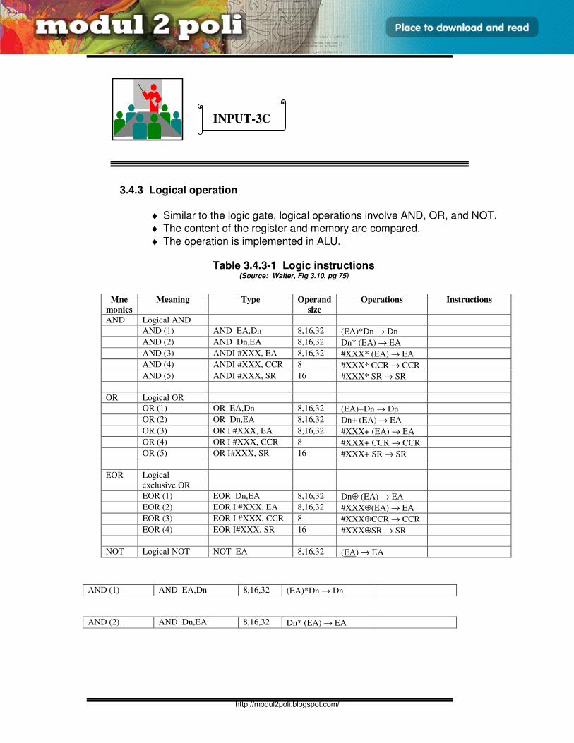
E3165 / UNIT 3 / 34
ASSEMBLY LANGUAGE
3.4.3 Logical operation
♦ Similar to the logic gate, logical operations involve AND, OR, and NOT.
♦ The content of the register and memory are compared.
♦ The operation is implemented in ALU.
Table 3.4.3-1 Logic instructions (Source: Walter, Fig 3.10, pg 75)
AND (1) AND EA,Dn 8,16,32 (EA)*Dn → Dn
AND (2) AND Dn,EA 8,16,32 Dn* (EA) → EA
INPUT-3C
Mne
monics
Meaning Type Operand
size
Operations Instructions
AND Logical AND
AND (1) AND EA,Dn 8,16,32 (EA)*Dn → Dn
AND (2) AND Dn,EA 8,16,32 Dn* (EA) → EA
AND (3) ANDI #XXX, EA 8,16,32 #XXX* (EA) → EA
AND (4) ANDI #XXX, CCR 8 #XXX* CCR → CCR
AND (5) ANDI #XXX, SR 16 #XXX* SR → SR
OR Logical OR
OR (1) OR EA,Dn 8,16,32 (EA)+Dn → Dn
OR (2) OR Dn,EA 8,16,32 Dn+ (EA) → EA
OR (3) OR I #XXX, EA 8,16,32 #XXX+ (EA) → EA
OR (4) OR I #XXX, CCR 8 #XXX+ CCR → CCR
OR (5) OR I#XXX, SR 16 #XXX+ SR → SR
EOR Logical
exclusive OR
EOR (1) EOR Dn,EA 8,16,32 Dn⊕ (EA) → EA
EOR (2) EOR I #XXX, EA 8,16,32 #XXX⊕(EA) → EA
EOR (3) EOR I #XXX, CCR 8 #XXX⊕CCR → CCR
EOR (4) EOR I#XXX, SR 16 #XXX⊕SR → SR
NOT Logical NOT NOT EA 8,16,32 (EA) → EA
http://modul2poli.blogspot.com/
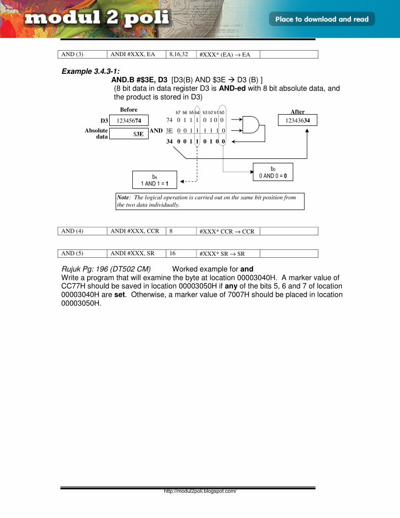
E3165 / UNIT 3 / 35
ASSEMBLY LANGUAGE
AND (3) ANDI #XXX, EA 8,16,32 #XXX* (EA) → EA
Example 3.4.3-1: AND.B #$3E, D3 [D3(B) AND $3E D3 (B) ]
(8 bit data in data register D3 is AND-ed with 8 bit absolute data, and the product is stored in D3)
AND (4) ANDI #XXX, CCR 8 #XXX* CCR → CCR
AND (5) ANDI #XXX, SR 16 #XXX* SR → SR
Rujuk Pg: 196 (DT502 CM) Worked example for and Write a program that will examine the byte at location 00003040H. A marker value of CC77H should be saved in location 00003050H if any of the bits 5, 6 and 7 of location 00003040H are set. Otherwise, a marker value of 7007H should be placed in location 00003050H.
D3 74 0 1 1 1 0 1 0 0
AND 3E 0 0 1 1 1 1 1 0
34 0 0 1 1 0 1 0 0
12345674
Before
$3E
12343634
Absolute data
After
b0 0 AND 0 = 0
b7 b6 b5 b4 b3 b2 b1 b0
b4 1 AND 1 = 1
Note: The logical operation is carried out on the same bit position from
the two data individually.
http://modul2poli.blogspot.com/
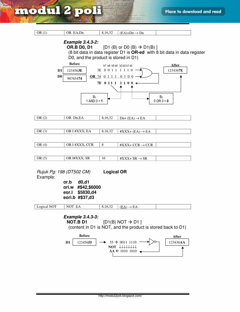
E3165 / UNIT 3 / 36
ASSEMBLY LANGUAGE
OR (1) OR EA,Dn 8,16,32 (EA)+Dn → Dn
Example 3.4.3-2: OR.B D0, D1 [D1 (B) or D0 (B) D1(B) ] (8 bit data in data register D1 is OR-ed with 8 bit data in data register D0, and the product is stored in D1)
OR (2) OR Dn,EA 8,16,32 Dn+ (EA) → EA
OR (3) OR I #XXX, EA 8,16,32 #XXX+ (EA) → EA
OR (4) OR I #XXX, CCR 8 #XXX+ CCR → CCR
OR (5) OR I#XXX, SR 16 #XXX+ SR → SR
Rujuk Pg: 198 (DT502 CM) Logical OR Example:
or.b d0,d1 ori.w #$42,$6000 eor.l $5830,d4 eori.b #$37,d3
Logical NOT NOT EA 8,16,32 (EA) → EA
Example 3.4.3-3:
NOT.B D1 [D1(B) NOT D1 ] (content in D1 is NOT, and the product is stored back to D1)
55 0011 1110
NOT ↓↓↓↓↓↓↓↓ AA 1010 1010
12345655
Before
123436AA D1
After
D1 3E 0 0 1 1 1 1 1 0
OR 74 0 1 1 1 0 1 0 0
7E 0 1 1 1 1 1 0 0
1234563E
Before
98765474
1234367E
D0
After
B0 0 OR 0 = 0
B3 1 AND 0 = 1
b7 b6 b5 b4 b3 b2 b1 b0
http://modul2poli.blogspot.com/
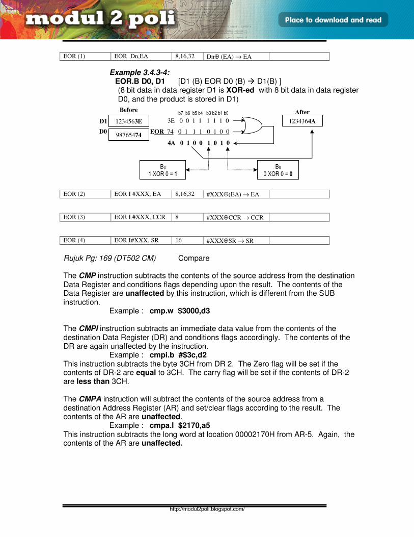
E3165 / UNIT 3 / 37
ASSEMBLY LANGUAGE
EOR (1) EOR Dn,EA 8,16,32 Dn⊕ (EA) → EA
Example 3.4.3-4: EOR.B D0, D1 [D1 (B) EOR D0 (B) D1(B) ] (8 bit data in data register D1 is XOR-ed with 8 bit data in data register D0, and the product is stored in D1)
EOR (2) EOR I #XXX, EA 8,16,32 #XXX⊕(EA) → EA
EOR (3) EOR I #XXX, CCR 8 #XXX⊕CCR → CCR
EOR (4) EOR I#XXX, SR 16 #XXX⊕SR → SR
Rujuk Pg: 169 (DT502 CM) Compare
The CMP instruction subtracts the contents of the source address from the destination Data Register and conditions flags depending upon the result. The contents of the Data Register are unaffected by this instruction, which is different from the SUB instruction.
Example : cmp.w $3000,d3 The CMPI instruction subtracts an immediate data value from the contents of the destination Data Register (DR) and conditions flags accordingly. The contents of the DR are again unaffected by the instruction.
Example : cmpi.b #$3c,d2 This instruction subtracts the byte 3CH from DR 2. The Zero flag will be set if the contents of DR-2 are equal to 3CH. The carry flag will be set if the contents of DR-2 are less than 3CH. The CMPA instruction will subtract the contents of the source address from a destination Address Register (AR) and set/clear flags according to the result. The contents of the AR are unaffected.
Example : cmpa.l $2170,a5 This instruction subtracts the long word at location 00002170H from AR-5. Again, the contents of the AR are unaffected.
D1 3E 0 0 1 1 1 1 1 0
EOR 74 0 1 1 1 0 1 0 0
4A 0 1 0 0 1 0 1 0
1234563E
Before
98765474
1234364A
D0
After
B0 0 XOR 0 = 0
B3 1 XOR 0 = 1
b7 b6 b5 b4 b3 b2 b1 b0
http://modul2poli.blogspot.com/
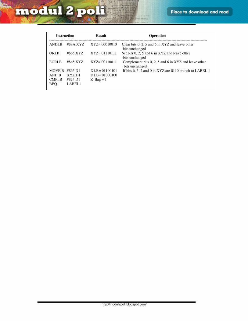
E3165 / UNIT 3 / 38
ASSEMBLY LANGUAGE
Instruction Result Operation
----------------------------------------------------------------------------------------------------------------------------
ANDI.B #$9A,XYZ XYZ= 00010010 Clear bits 0, 2, 5 and 6 in XYZ and leave other
bits unchanged
ORI.B #$65,XYZ XYZ= 01110111 Set bits 0, 2, 5 and 6 in XYZ and leave other
bits unchanged
EORI.B #$65,XYZ XYZ= 00110011 Complement bits 0, 2, 5 and 6 in XYZ and leave other
bits unchanged
MOVE.B #$65,D1 D1.B= 01100101 If bits 6, 5, 2 and 0 in XYZ are 0110 branch to LABEL 1
AND.B XYZ,D1 D1.B= 01000100
CMPI.B #$24,D1 Z flag = 1
BEQ LABEL1
http://modul2poli.blogspot.com/
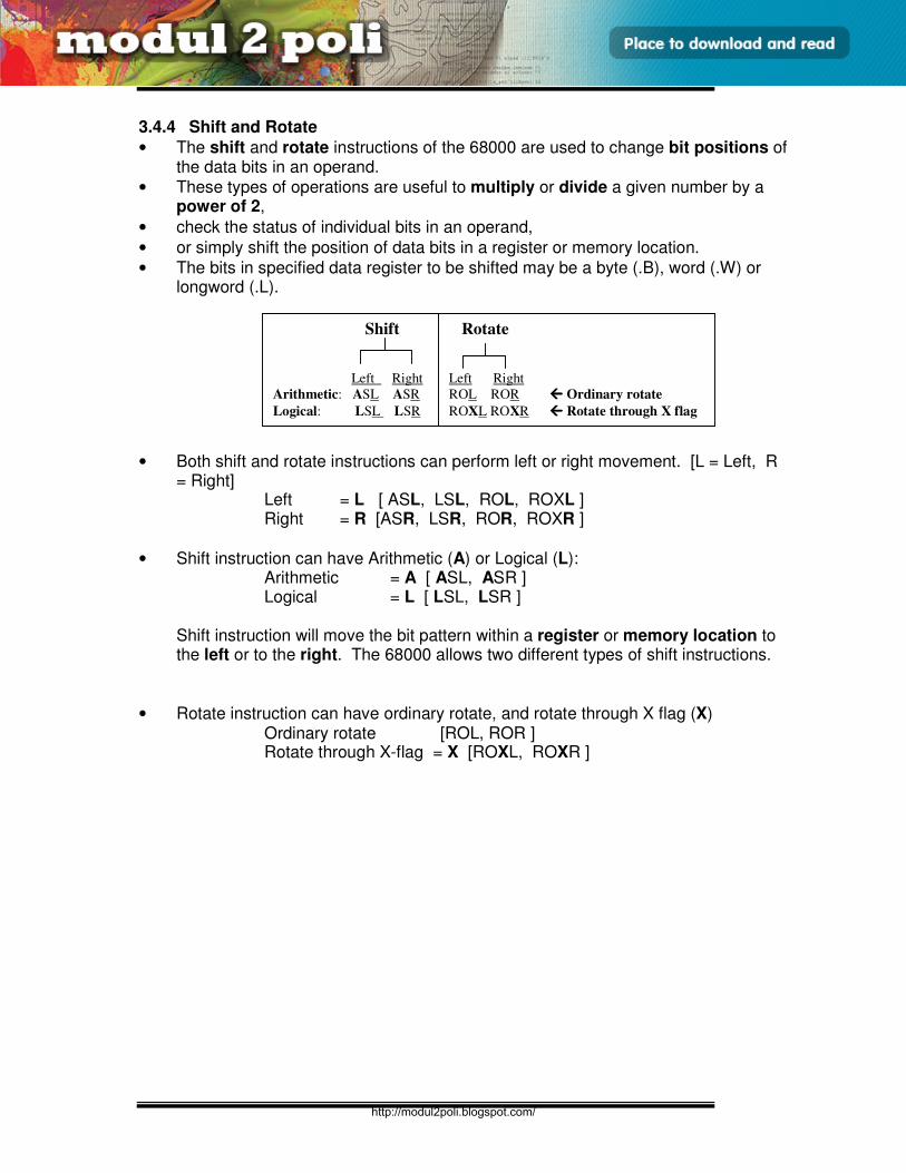
E3165 / UNIT 3 / 39
ASSEMBLY LANGUAGE
3.4.4 Shift and Rotate
• The shift and rotate instructions of the 68000 are used to change bit positions of the data bits in an operand.
• These types of operations are useful to multiply or divide a given number by a power of 2,
• check the status of individual bits in an operand,
• or simply shift the position of data bits in a register or memory location.
• The bits in specified data register to be shifted may be a byte (.B), word (.W) or longword (.L).
• Both shift and rotate instructions can perform left or right movement. [L = Left, R = Right]
Left = L [ ASL, LSL, ROL, ROXL ] Right = R [ASR, LSR, ROR, ROXR ]
• Shift instruction can have Arithmetic (A) or Logical (L): Arithmetic = A [ ASL, ASR ] Logical = L [ LSL, LSR ]
Shift instruction will move the bit pattern within a register or memory location to the left or to the right. The 68000 allows two different types of shift instructions.
• Rotate instruction can have ordinary rotate, and rotate through X flag (X) Ordinary rotate [ROL, ROR ] Rotate through X-flag = X [ROXL, ROXR ]
Shift
Left Right
Arithmetic: ASL ASR
Logical: LSL LSR
Rotate
Left Right
ROL ROR Ordinary rotate
ROXL ROXR Rotate through X flag
http://modul2poli.blogspot.com/
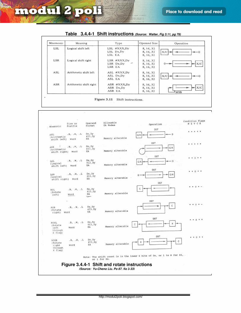
E3165 / UNIT 3 / 40
ASSEMBLY LANGUAGE
Table 3.4.4-1 Shift instructions (Source: Walter, Fig 3.11, pg 79)
Figure 3.4.4-1 Shift and rotate instructions (Source: Yu-Cheng Liu, Pg 87, fig 3-33)
http://modul2poli.blogspot.com/
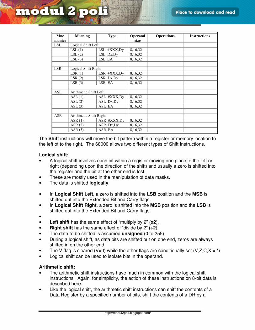
E3165 / UNIT 3 / 41
ASSEMBLY LANGUAGE
The Shift instructions will move the bit pattern within a register or memory location to the left ot to the right. The 68000 allows two different types of Shift Instructions. Logical shift:
• A logical shift involves each bit within a register moving one place to the left or right (depending upon the direction of the shift) and usually a zero is shifted into the register and the bit at the other end is lost.
• These are mostly used in the manipulation of data masks.
• The data is shifted logically.
• In Logical Shift Left, a zero is shifted into the LSB position and the MSB is shifted out into the Extended Bit and Carry flags.
• In Logical Shift Right, a zero is shifted into the MSB position and the LSB is shifted out into the Extended Bit and Carry flags.
•
• Left shift has the same effect of “multiply by 2” (x2).
• Right shift has the same effect of “divide by 2” (÷÷÷÷2).
• The data to be shifted is assumed unsigned (0 to 255)
• During a logical shift, as data bits are shifted out on one end, zeros are always shifted in on the other end.
• The V flag is cleared (V=0) while the other flags are conditionally set (V,Z,C,X = *).
• Logical shift can be used to isolate bits in the operand.
Arithmetic shift:
• The arithmetic shift instructions have much in common with the logical shift instructions. Again, for simplicity, the action of these instructions on 8-bit data is described here.
• Like the logical shift, the arithmetic shift instructions can shift the contents of a Data Register by a specified number of bits, shift the contents of a DR by a
Mne
monics
Meaning Type Operand
size
Operations Instructions
LSL Logical Shift Left
LSL (1) LSL #XXX,Dy 8,16,32
LSL (2) LSL Dx,Dy 8,16,32
LSL (3) LSL EA 8,16,32
LSR Logical Shift Right
LSR (1) LSR #XXX,Dy 8,16,32
LSR (2) LSR Dx,Dy 8,16,32
LSR (3) LSR EA 8,16,32
ASL Arithmetic Shift Left
ASL (1) ASL #XXX,Dy 8,16,32
ASL (2) ASL Dx,Dy 8,16,32
ASL (3) ASL EA 8,16,32
ASR Arithmetic Shift Right
ASR (1) ASR #XXX,Dy 8,16,32
ASR (2) ASR Dx,Dy 8,16,32
ASR (3) ASR EA 8,16,32
http://modul2poli.blogspot.com/
E3165 / UNIT 3 / 42
ASSEMBLY LANGUAGE
number of bits specified by the another DR, or shift the contents of a memory location by 1 bit.
• These are mostly used in signed arithmetic.
• The data is shifted arithmetically.
• In Arithmetic Shift Left, a zero is shifted into the LSB. The MSB is shifted out into the Extended Bit and Carry flags.
• In Arithmetic Shift Right, each bit is shifted to right but MSB is copied back to itself. The LSB is shifted out into the Extended Bit and Carry flags.
• Left shift has the same effect of “multiply by 2” (x2).
• Right shift has the same effect of “divide by 2” (÷÷÷÷2).
• The data to be shifted is assumed signed (0 to127, -1 to -128)
• These instructions preserve the sign of the original operand while being shifted.
• The ASR instruction extends the sign bit after each right shift operation.
• Therefore, this instruction may be used to divide an operand by 2N, where N is
the shift count. [÷÷÷÷2N]
• However, when the operand is negative, the ASR may not produce the same result as the quotient yielded from the DIVU instruction.
• The ASL sets the V flag to indicate an overflow whenever the sign bit has been changed by the left shift operation. Therefore, shifting an operand to the left by N bits is equivalent to the signed multiplication of the operand by 2N. [ x2N ]
Both shift instructions will affect the Carry (C) and Extended bit (X) flags. The X flag is a duplicate of C flag but is not affected by all the shift instructions. The X flag is only used in multiple precision arithmetic.
http://modul2poli.blogspot.com/
E3165 / UNIT 3 / 43
ASSEMBLY LANGUAGE
Rotate:
• These Rotate instructions are similar to shift instructions, except that instead of one bit being lost and a zero shifting in, the last bit is shifted back in at the beginning.
• The rotate instructions perform circular shift operations.
• Bits shifted out of an operand are not lost as in the shift instructions, but are rotated back into the other end of the operand.
• Rotate Left : Each bit is shifted to the left. The MSB is shifted out into the LSB position and into the Carry flag.
• Rotate Right : Each bit is shifted to the right. The LSB is shifted out into both the MSB position and into the Carry flag.
• The ROXL and ROXR instructions perform rotate operations through the X-flag.
• On the other hand, the ROL and ROR instructions do not include the X flag in the circle of rotation.
• The ROXL and ROXR instructions are essential in implementing shift and rotate operations for operands with , as required in some applications such as unsigned division of 64 bits by 32 bits, the 64-bit dividend needs to be shifted to the left as a whole during each iteration.
• Rotate Left With Extend (ROXL) : Each bit is shifted to the left, through the Extended bit flag. The MSB is shifted out into both the Extended Bit and Carry flags. The Extended bit flag is shifted into the LSB position.
• Rotate Right With Extend (ROXR) : Each bit is shifted to the right, through the Extended bit flag. The LSB is shifted out into both the Extended Bit and Carry flags. The Extended bit flag is shifted into the MSB position.
• Shift and Rotate instructions can be used for generating output bit sequences for microprocessor control applications. They could also be used in multiplication and division algorithm, since shifting left by one place gives multiplication by 2 (in the same way that adding a 0 to the right hand side of a decimal number gives multiplication by 10). Similarly, shifting right gives division by 2.
http://modul2poli.blogspot.com/
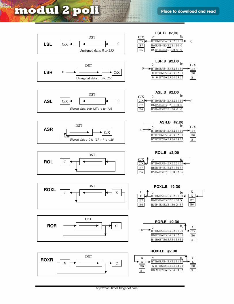
E3165 / UNIT 3 / 44
ASSEMBLY LANGUAGE
C/X 0
DST
LSL
Unsigned data: 0 to 255
C/X 0
DST
LSR
Unsigned data : 0 to 255
C/X 0
DST
ASL
Signed data: 0 to 127 ; -1 to -128
C/X
DST ASR
MSB Signed data : 0 to 127 ; -1 to -128
C
DST
ROL
C
DST ROXL
X
C
DST
ROR
C
DST ROXR
X
B7
B6
B5
B4
B3
B2
B1
B0
b7 b0
C/X
C/X 0
B6
B5
B4
B3
B2
B1
B0
0
B7
B5
B4
B3
B2
B1
B0
0
0
B6
B7
B6
B5
B4
B3
B2
B1
B0
b7 b0
C/X
C/X 0
0
B7
B6
B5
B4
B3
B2
B1
B0
0
0
B7
B6
B5
B4
B3
B2
B1
B7
B6
B5
B4
B3
B2
B1
B0
b7 b0
C/X
C/X
0 B6
B5
B4
B3
B2
B1
B0
0
B7
B5
B4
B3
B2
B1
B0
0
0
B6
B7
B6
B5
B4
B3
B2
B1
B0
b7 b0
C/X
C/X b7
B7
B7
B6
B5
B4
B3
B2
B1
B0
B7
B7 B7
B6
B5
B4
B3
B2
B1
B7
B6
B5
B4
B3
B2
B1
B0
b7 b0 C/X
C/X
B6
B5
B4
B3
B2
B1
B0
B7
B7
B5
B4
B3
B2
B1
B0
B7
B6
B6
B7
B6
B5
B4
B3
B2
B1
B0
b7 b0 C
C
B6
B5
B4
B3
B2
B1
B0
X
B7
B5
B4
B3
B2
B1
B0
X
B7
B6
X
X
B7
B6
B7
B6
B5
B4
B3
B2
B1
B0
b7 b0
C/X
C b0
B0
B7
B6
B5
B4
B3
B2
B1
B0
B1
B0 B7
B6
B5
B4
B3
B2
B1
B7
B6
B5
B4
B3
B2
B1
B0
b7 b0 C
C
X
B7
B6
B5
B4
B3
B2
B1
B0
B0
X B7
B6
B5
B4
B3
B2
B1
X
X
B0
B1
LSL.B #2,D0
LSR.B #2,D0
ASL.B #2,D0
ASR.B #2,D0
ROL.B #2,D0
ROXL.B #2,D0
ROR.B #2,D0
ROXR.B #2,D0
http://modul2poli.blogspot.com/
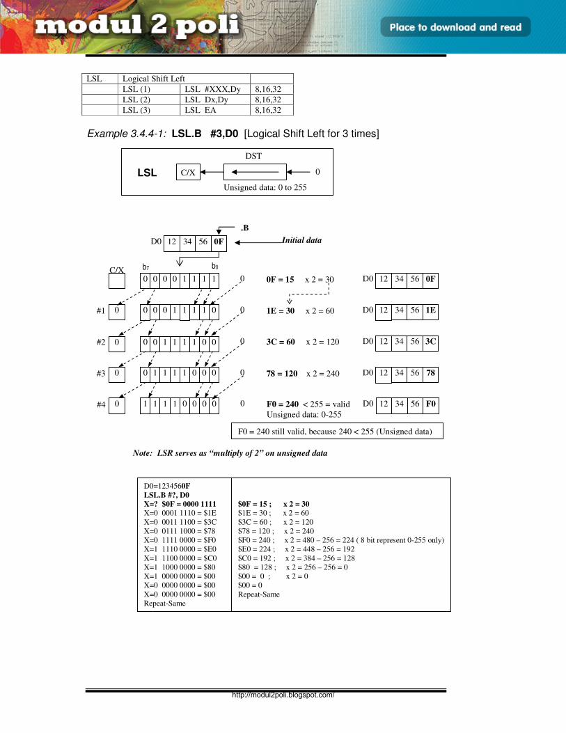
E3165 / UNIT 3 / 45
ASSEMBLY LANGUAGE
LSL Logical Shift Left
LSL (1) LSL #XXX,Dy 8,16,32
LSL (2) LSL Dx,Dy 8,16,32
LSL (3) LSL EA 8,16,32
Example 3.4.4-1: LSL.B #3,D0 [Logical Shift Left for 3 times]
C/X 0
DST
LSL
Unsigned data: 0 to 255
12 34 56 D0 0F
0 0 0 1 1 1 1 0 0 0 1E = 30 x 2 = 60
3C = 60 x 2 = 120
78 = 120 x 2 = 240
.B
Initial data
0 0 1 1 1 1 0 0 0 0
0 1 1 1 1 0 0 0 0 0
12 34 56 D0 1E
D0 12 34 56 3C
12 34 56 D0 78
0 0 0 0 1 1 1 1
b7 b0
C/X
0 0F = 15 x 2 = 30 12 34 56 D0 0F
#1
#2
#3
Note: LSR serves as “multiply of 2” on unsigned data
F0 = 240 < 255 = valid
Unsigned data: 0-255
1 1 1 1 0 0 0 0 0 0 12 34 56 D0 F0 #4
F0 = 240 still valid, because 240 < 255 (Unsigned data)
D0=1234560F
LSL.B #?, D0
X=? $0F = 0000 1111
X=0 0001 1110 = $1E
X=0 0011 1100 = $3C
X=0 0111 1000 = $78
X=0 1111 0000 = $F0
X=1 1110 0000 = $E0
X=1 1100 0000 = $C0
X=1 1000 0000 = $80
X=1 0000 0000 = $00
X=0 0000 0000 = $00
X=0 0000 0000 = $00
Repeat-Same
$0F = 15 ; x 2 = 30
$1E = 30 ; x 2 = 60
$3C = 60 ; x 2 = 120
$78 = 120 ; x 2 = 240
$F0 = 240 ; x 2 = 480 – 256 = 224 ( 8 bit represent 0-255 only)
$E0 = 224 ; x 2 = 448 – 256 = 192
$C0 = 192 ; x 2 = 384 – 256 = 128
$80 = 128 ; x 2 = 256 – 256 = 0
$00 = 0 ; x 2 = 0
$00 = 0
Repeat-Same
http://modul2poli.blogspot.com/
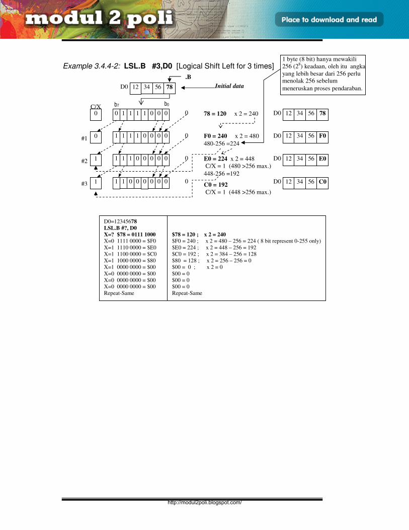
E3165 / UNIT 3 / 46
ASSEMBLY LANGUAGE
Example 3.4.4-2: LSL.B #3,D0 [Logical Shift Left for 3 times]
12 34 56 D0 78
0 1 1 1 1 0 0 0 0 0 78 = 120 x 2 = 240
F0 = 240 x 2 = 480
480-256 =224
E0 = 224 x 2 = 448
C/X = 1 (480 >256 max.)
448-256 =192
.B
Initial data
1 1 1 1 0 0 0 0 0 0
1 1 1 0 0 0 0 0 1 0
12 34 56 D0 78
D0 12 34 56 F0
12 34 56 D0 E0
b7 b0 C/X
1 1 0 0 0 0 0 0 1 0 C0 = 192
C/X = 1 (448 >256 max.)
12 34 56 D0 C0
#1
#3
#2
1 byte (8 bit) hanya mewakili
256 (28) keadaan, oleh itu angka
yang lebih besar dari 256 perlu
menolak 256 sebelum
meneruskan proses pendaraban.
D0=12345678
LSL.B #?, D0
X=? $78 = 0111 1000
X=0 1111 0000 = $F0
X=1 1110 0000 = $E0
X=1 1100 0000 = $C0
X=1 1000 0000 = $80
X=1 0000 0000 = $00
X=0 0000 0000 = $00
X=0 0000 0000 = $00
X=0 0000 0000 = $00
Repeat-Same
$78 = 120 ; x 2 = 240
$F0 = 240 ; x 2 = 480 – 256 = 224 ( 8 bit represent 0-255 only)
$E0 = 224 ; x 2 = 448 – 256 = 192
$C0 = 192 ; x 2 = 384 – 256 = 128
$80 = 128 ; x 2 = 256 – 256 = 0
$00 = 0 ; x 2 = 0
$00 = 0
$00 = 0
$00 = 0
Repeat-Same
http://modul2poli.blogspot.com/
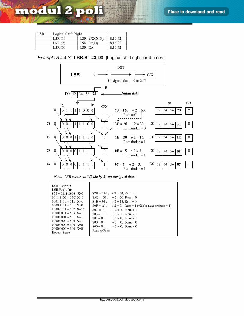
E3165 / UNIT 3 / 47
ASSEMBLY LANGUAGE
LSR Logical Shift Right
LSR (1) LSR #XXX,Dy 8,16,32
LSR (2) LSR Dx,Dy 8,16,32
LSR (3) LSR EA 8,16,32
Example 3.4.4-3: LSR.B #3,D0 [Logical shift right for 4 times]
Note: LSR serves as “divide by 2” on unsigned data
12 34 56 D0 78
0 1 1 1 1 0 0 0
b7 b0
C/X
0 0 1 1 1 1 0 0 0
0
0
0 0 0 1 1 1 1 0 0 0
0 0 0 0 1 1 1 1 0 0
78 = 120 ÷ 2 = 60,
Rem = 0
3C = 60 ÷ 2 = 30,
Remainder = 0
1E = 30 ÷ 2 = 15,
Remainder = 1
0F = 15 ÷ 2 = 7,
Remainder = 1
.B
Initial data
#1
#2
#3
12 34 56
D0
78
12 34 56 D0 3C
12 34 56 D0 1E
12 34 56 D0 0F
?
C/X
0
0
0
0 0 0 0 0 1 1 1 0 1 #4 07 = 7 ÷ 2 = 3,
Remainder = 1
12 34 56 D0 07 1
C/X 0
DST
LSR
Unsigned data : 0 to 255
D0=12345678
LSR.B #?, D0
$78 = 0111 1000 X=?
0011 1100 = $3C X=0
0001 1110 = $1E X=0
0000 1111 = $0F X=0
0000 0111 = $07 X=1*
0000 0011 = $03 X=1
0000 0001 = $01 X=1
0000 0000 = $00 X=1
0000 0000 = $00 X=0
0000 0000 = $00 X=0
Repeat-Same
$78 = 120 ; ÷ 2 = 60, Rem = 0
$3C = 60 ; ÷ 2 = 30, Rem = 0
$1E = 30 ; ÷ 2 = 15, Rem = 0
$0F = 15 ; ÷ 2 = 7, Rem = 1 (*X for next process = 1)
$07 = 7 ; ÷ 2 = 3, Rem = 1
$03 = 1 ; ÷ 2 = 1, Rem = 1
$01 = 0 ; ÷ 2 = 0, Rem = 1
$00 = 0 ; ÷ 2 = 0, Rem = 0
$00 = 0 ; ÷ 2 = 0, Rem = 0
Repeat-Same
http://modul2poli.blogspot.com/
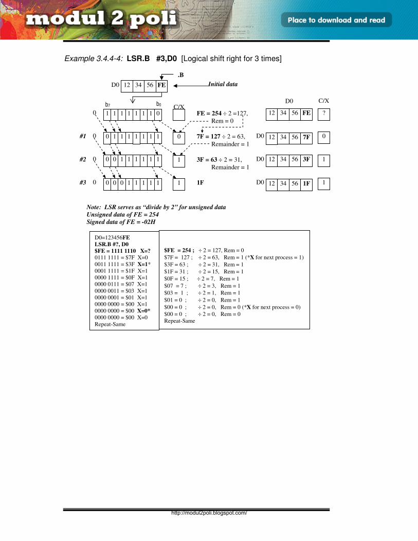
E3165 / UNIT 3 / 48
ASSEMBLY LANGUAGE
Example 3.4.4-4: LSR.B #3,D0 [Logical shift right for 3 times]
Note: LSR serves as “divide by 2” for unsigned data
Unsigned data of FE = 254
Signed data of FE = -02H
12 34 56 D0 FE
1 1 1 1 1 1 1 0
b7 b0
C/X
0 1 1 1 1 1 1 1 0
0
0
0 0 1 1 1 1 1 1 0 1
0 0 0 1 1 1 1 1 0 1
FE = 254 ÷ 2 =127,
Rem = 0
7F = 127 ÷ 2 = 63,
Remainder = 1
3F = 63 ÷ 2 = 31,
Remainder = 1
1F
.B
Initial data
#1
#2
#3
12 34 56
D0
FE
12 34 56 D0 7F
12 34 56 D0 3F
12 34 56 D0 1F
?
C/X
0
1
1
D0=123456FE
LSR.B #?, D0
$FE = 1111 1110 X=?
0111 1111 = $7F X=0
0011 1111 = $3F X=1*
0001 1111 = $1F X=1
0000 1111 = $0F X=1
0000 0111 = $07 X=1
0000 0011 = $03 X=1
0000 0001 = $01 X=1
0000 0000 = $00 X=1
0000 0000 = $00 X=0*
0000 0000 = $00 X=0
Repeat-Same
$FE = 254 ; ÷ 2 = 127, Rem = 0
$7F = 127 ; ÷ 2 = 63, Rem = 1 (*X for next process = 1)
$3F = 63 ; ÷ 2 = 31, Rem = 1
$1F = 31 ; ÷ 2 = 15, Rem = 1
$0F = 15 ; ÷ 2 = 7, Rem = 1
$07 = 7 ; ÷ 2 = 3, Rem = 1
$03 = 1 ; ÷ 2 = 1, Rem = 1
$01 = 0 ; ÷ 2 = 0, Rem = 1
$00 = 0 ; ÷ 2 = 0, Rem = 0 (*X for next process = 0)
$00 = 0 ; ÷ 2 = 0, Rem = 0
Repeat-Same
http://modul2poli.blogspot.com/
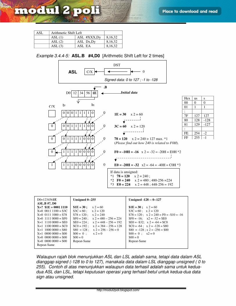
E3165 / UNIT 3 / 49
ASSEMBLY LANGUAGE
ASL Arithmetic Shift Left
ASL (1) ASL #XXX,Dy 8,16,32
ASL (2) ASL Dx,Dy 8,16,32
ASL (3) ASL EA 8,16,32
Example 3.4.4-5: ASL.B #4,D0 [Arithmetic Shift Left for 2 times]
Walaupun rajah blok menunjukkan ASL dan LSL adalah sama, tetapi data dalam ASL dianggap signed (-128 to 0 to 127), manakala data dalam LSL dianggap unsigned ( 0 to 255). Contoh di atas menunjukkan walaupun data terhasil adalah sama untuk kedua-dua ASL dan LSL, tetapi keputusan operasi yang terhasil betul untuk kedua-dua data sign atau unsigned.
12 34 56 D0 1E
0 1 1 1 1 0 0 0
b7 b0
0
C/X
0 78 = 120 x 2 = 240 > 127 max. *1
(Please find out how 240 is related to F0H).
F0 = -10H = -16 x 2 = -32 = -20H = E0H *2
E0 = -20H = -32 x2 = -64 = -40H = C0H *3
.B
Initial data
1 1 1 1 0 0 0 0 0 0
1 1 1 0 0 0 0 0 1 0
0 0 1 1 1 1 0 0 0 0
0 0 0 1 1 1 1 0 0
3C = 60 x 2 = 120
1E = 30 x 2 = 60
If data is unsigned:
*1 78 = 120 x 2 = 240 ;
*2 F0 = 240 x 2 = 480 ; 480-256 =224
*3 E0 = 224 x 2 = 448 ; 448-256 = 192
C/X 0
DST
ASL
Signed data: 0 to 127 ; -1 to -128
D0=1234561E
ASL.B #?, D0
X=? $1E = 0001 1110
X=0 0011 1100 = $3C
X=0 0111 1000 = $78
X=0 1111 0000 = $F0
X=1 1110 0000 = $E0
X=1 1100 0000 = $C0
X=1 1000 0000 = $80
X=1 0000 0000 = $00
X=0 0000 0000 = $00
X=0 0000 0000 = $00
Repeat-Same
Unsigned 0--255
$1E = 30 ; x 2 = 60
$3C = 60 ; x 2 = 120
$78 = 120 ; x 2 = 240
$F0 = 240 ; x 2 = 480 – 256 = 224
$E0 = 224 ; x 2 = 448 – 256 = 192
$C0 = 192 ; x 2 = 384 – 256 = 128
$80 = 128 ; x 2 = 256 – 256 = 0
$00 = 0 ; x 2 = 0
$00 = 0
Repeat-Same
Hex us s
00 0 0
01 1 1
:
7F 127 127
80 128 -128
81 129 -127
:
FE 254 -2
FF 255 -1
Unsigned -128 -- 0--127
$1E = 30 ; x 2 = 60
$3C = 60 ; x 2 = 120
$78 = 120 ; x 2 = 240 = F0 = -$10 = -16
$F0 = -16; x2 = -32 = $E0
$E0 = -$32; x 2 = -64 = $C0
$C0 = -64 ; x 2 = -128 = $80
$80 = -128 ; x 2 = -256 = $00
$00 = 0 ; x2 = 0
$00 = 0
Repeat-Same
http://modul2poli.blogspot.com/
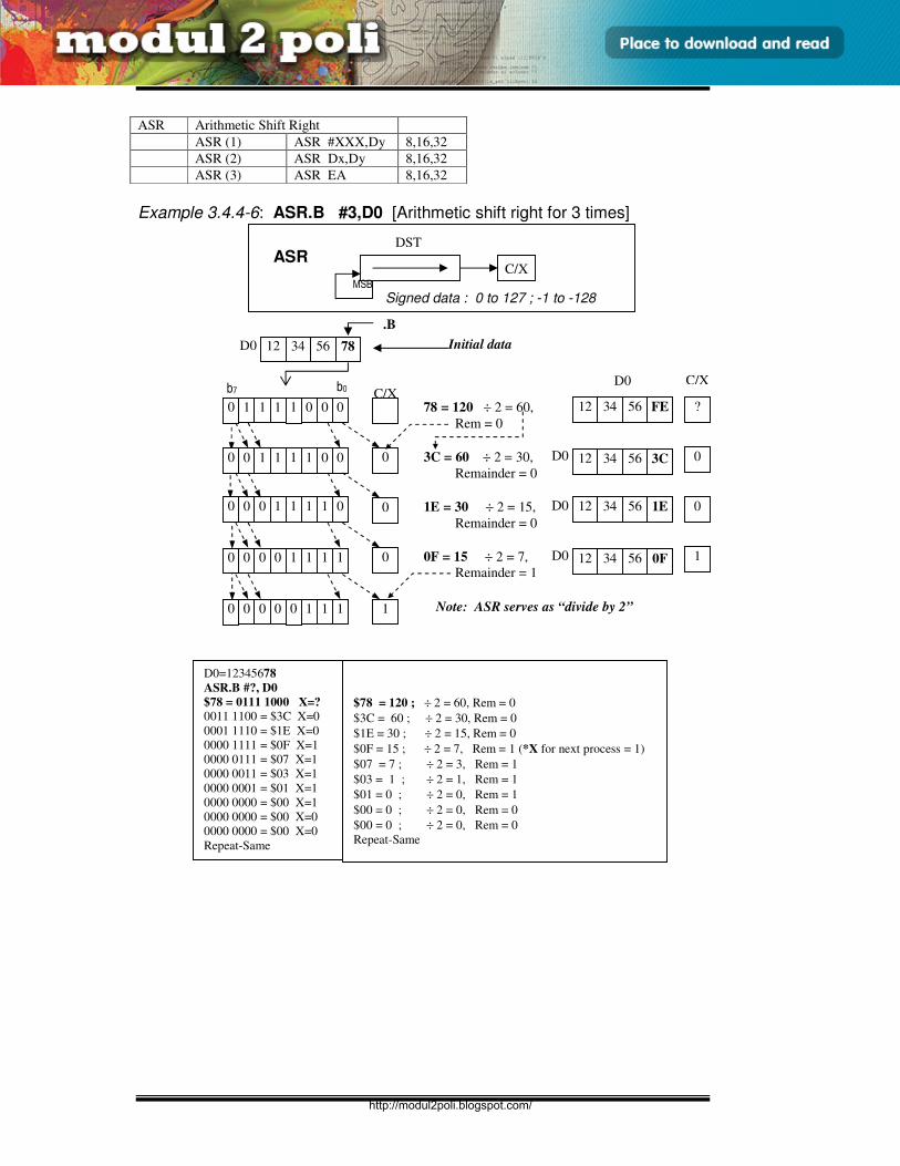
E3165 / UNIT 3 / 50
ASSEMBLY LANGUAGE
ASR Arithmetic Shift Right
ASR (1) ASR #XXX,Dy 8,16,32
ASR (2) ASR Dx,Dy 8,16,32
ASR (3) ASR EA 8,16,32
Example 3.4.4-6: ASR.B #3,D0 [Arithmetic shift right for 3 times]
12 34 56 D0 78
0 1 1 1 1 0 0 0
b7 b0
C/X
0 0 1 1 1 1 0 0 0
0 0 0 1 1 1 1 0 0
0 0 0 0 1 1 1 1 0
78 = 120 ÷ 2 = 60,
Rem = 0
3C = 60 ÷ 2 = 30,
Remainder = 0
1E = 30 ÷ 2 = 15,
Remainder = 0
0F = 15 ÷ 2 = 7,
Remainder = 1
.B
Initial data
12 34 56
D0
FE
12 34 56 D0 3C
12 34 56 D0 1E
12 34 56 D0 0F
?
C/X
0
1
0
0 0 0 0 0 1 1 1 1 Note: ASR serves as “divide by 2”
C/X
DST ASR
MSB
Signed data : 0 to 127 ; -1 to -128
D0=12345678
ASR.B #?, D0
$78 = 0111 1000 X=?
0011 1100 = $3C X=0
0001 1110 = $1E X=0
0000 1111 = $0F X=1
0000 0111 = $07 X=1
0000 0011 = $03 X=1
0000 0001 = $01 X=1
0000 0000 = $00 X=1
0000 0000 = $00 X=0
0000 0000 = $00 X=0
Repeat-Same
$78 = 120 ; ÷ 2 = 60, Rem = 0
$3C = 60 ; ÷ 2 = 30, Rem = 0
$1E = 30 ; ÷ 2 = 15, Rem = 0
$0F = 15 ; ÷ 2 = 7, Rem = 1 (*X for next process = 1)
$07 = 7 ; ÷ 2 = 3, Rem = 1
$03 = 1 ; ÷ 2 = 1, Rem = 1
$01 = 0 ; ÷ 2 = 0, Rem = 1
$00 = 0 ; ÷ 2 = 0, Rem = 0
$00 = 0 ; ÷ 2 = 0, Rem = 0
Repeat-Same
http://modul2poli.blogspot.com/
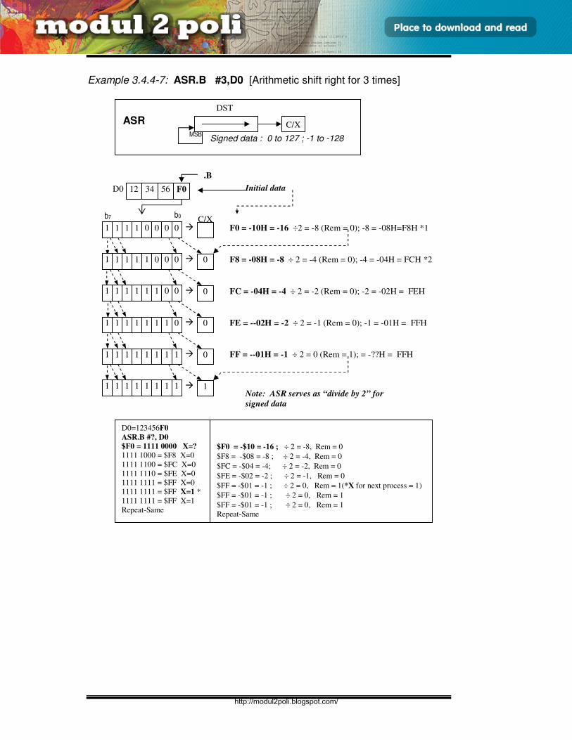
E3165 / UNIT 3 / 51
ASSEMBLY LANGUAGE
Example 3.4.4-7: ASR.B #3,D0 [Arithmetic shift right for 3 times]
12 34 56 D0 F0
1 1 1 1 0 0 0 0
b7 b0
C/X
1 1 1 1 1 0 0 0 0
1 1 1 1 1 1 0 0 0
1 1 1 1 1 1 1 0 0
F0 = -10H = -16 ÷2 = -8 (Rem = 0); -8 = -08H=F8H *1
FC = -04H = -4 ÷ 2 = -2 (Rem = 0); -2 = -02H = FEH
FE = --02H = -2 ÷ 2 = -1 (Rem = 0); -1 = -01H = FFH
.B
Initial data
Note: ASR serves as “divide by 2” for
signed data
1 1 1 1 1 1 1 1 0 FF = --01H = -1 ÷ 2 = 0 (Rem = 1); = -??H = FFH
1 1 1 1 1 1 1 1 1
F8 = -08H = -8 ÷ 2 = -4 (Rem = 0); -4 = -04H = FCH *2
C/X
DST
ASR
MSB Signed data : 0 to 127 ; -1 to -128
D0=123456F0
ASR.B #?, D0
$F0 = 1111 0000 X=?
1111 1000 = $F8 X=0
1111 1100 = $FC X=0
1111 1110 = $FE X=0
1111 1111 = $FF X=0
1111 1111 = $FF X=1 *
1111 1111 = $FF X=1
Repeat-Same
$F0 = -$10 = -16 ; ÷ 2 = -8, Rem = 0
$F8 = -$08 = -8 ; ÷ 2 = -4, Rem = 0
$FC = -$04 = -4; ÷ 2 = -2, Rem = 0
$FE = -$02 = -2 ; ÷ 2 = -1, Rem = 0
$FF = -$01 = -1 ; ÷ 2 = 0, Rem = 1(*X for next process = 1)
$FF = -$01 = -1 ; ÷ 2 = 0, Rem = 1
$FF = -$01 = -1 ; ÷ 2 = 0, Rem = 1
Repeat-Same
http://modul2poli.blogspot.com/
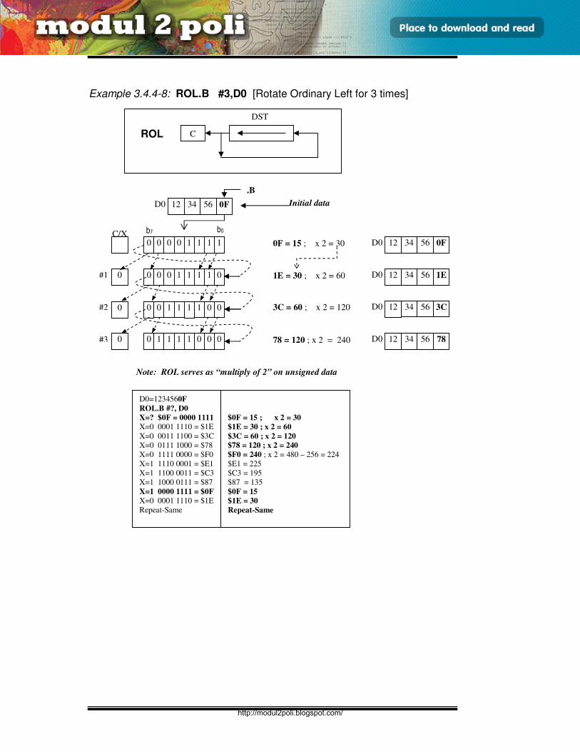
E3165 / UNIT 3 / 52
ASSEMBLY LANGUAGE
Example 3.4.4-8: ROL.B #3,D0 [Rotate Ordinary Left for 3 times]
12 34 56 D0 0F
0 0 0 1 1 1 1 0 0 1E = 30 ; x 2 = 60
3C = 60 ; x 2 = 120
78 = 120 ; x 2 = 240
.B
Initial data
0 0 1 1 1 1 0 0 0
0 1 1 1 1 0 0 0 0
12 34 56 D0 1E
D0 12 34 56 3C
12 34 56 D0 78
0 0 0 0 1 1 1 1
b7 b0
C/X
0F = 15 ; x 2 = 30 12 34 56 D0 0F
#1
#2
#3
Note: ROL serves as “multiply of 2” on unsigned data
C
DST
ROL
D0=1234560F
ROL.B #?, D0
X=? $0F = 0000 1111
X=0 0001 1110 = $1E
X=0 0011 1100 = $3C
X=0 0111 1000 = $78
X=0 1111 0000 = $F0
X=1 1110 0001 = $E1
X=1 1100 0011 = $C3
X=1 1000 0111 = $87
X=1 0000 1111 = $0F
X=0 0001 1110 = $1E
Repeat-Same
$0F = 15 ; x 2 = 30
$1E = 30 ; x 2 = 60
$3C = 60 ; x 2 = 120
$78 = 120 ; x 2 = 240
$F0 = 240 ; x 2 = 480 – 256 = 224
$E1 = 225
$C3 = 195
$87 = 135
$0F = 15
$1E = 30
Repeat-Same
http://modul2poli.blogspot.com/
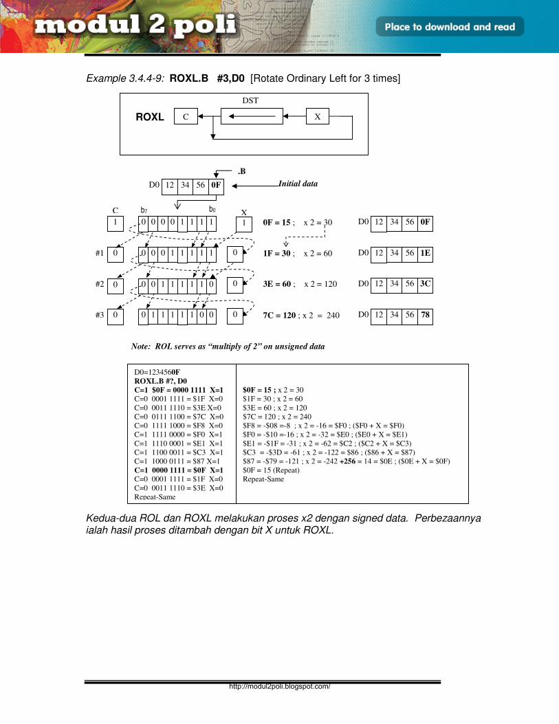
E3165 / UNIT 3 / 53
ASSEMBLY LANGUAGE
Example 3.4.4-9: ROXL.B #3,D0 [Rotate Ordinary Left for 3 times]
Kedua-dua ROL dan ROXL melakukan proses x2 dengan signed data. Perbezaannya ialah hasil proses ditambah dengan bit X untuk ROXL.
12 34 56 D0 0F
0 0 0 1 1 1 1 1 0 1F = 30 ; x 2 = 60
3E = 60 ; x 2 = 120
7C = 120 ; x 2 = 240
.B
Initial data
0 0 1 1 1 1 1 0 0
0 1 1 1 1 1 0 0 0
12 34 56 D0 1E
D0 12 34 56 3C
12 34 56 D0 78
0 0 0 0 1 1 1 1
b7 b0
1
C
0F = 15 ; x 2 = 30 12 34 56 D0 0F
#1
#2
#3
Note: ROL serves as “multiply of 2” on unsigned data
D0=1234560F
ROXL.B #?, D0
C=1 $0F = 0000 1111 X=1
C=0 0001 1111 = $1F X=0
C=0 0011 1110 = $3E X=0
C=0 0111 1100 = $7C X=0
C=0 1111 1000 = $F8 X=0
C=1 1111 0000 = $F0 X=1
C=1 1110 0001 = $E1 X=1
C=1 1100 0011 = $C3 X=1
C=1 1000 0111 = $87 X=1
C=1 0000 1111 = $0F X=1
C=0 0001 1111 = $1F X=0
C=0 0011 1110 = $3E X=0
Repeat-Same
$0F = 15 ; x 2 = 30
$1F = 30 ; x 2 = 60
$3E = 60 ; x 2 = 120
$7C = 120 ; x 2 = 240
$F8 = -$08 =-8 ; x 2 = -16 = $F0 ; ($F0 + X = $F0)
$F0 = -$10 =-16 ; x 2 = -32 = $E0 ; ($E0 + X = $E1)
$E1 = -$1F = -31 ; x 2 = -62 = $C2 ; ($C2 + X = $C3)
$C3 = -$3D = -61 ; x 2 = -122 = $86 ; ($86 + X = $87)
$87 = -$79 = -121 ; x 2 = -242 +256 = 14 = $0E ; ($0E + X = $0F)
$0F = 15 (Repeat)
Repeat-Same
C
DST
ROXL X
1
X
0
0
0
http://modul2poli.blogspot.com/
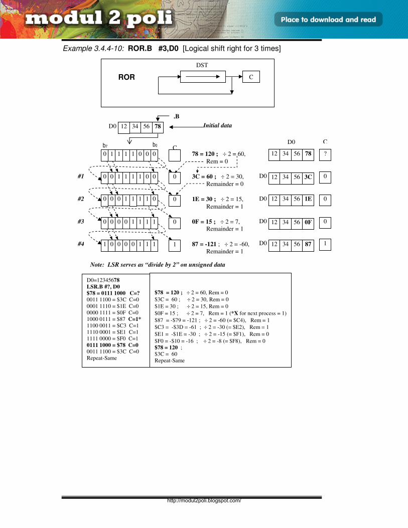
E3165 / UNIT 3 / 54
ASSEMBLY LANGUAGE
Example 3.4.4-10: ROR.B #3,D0 [Logical shift right for 3 times] `
Note: LSR serves as “divide by 2” on unsigned data
12 34 56 D0 78
0 1 1 1 1 0 0 0
b7 b0
C
0 0 1 1 1 1 0 0 0
0 0 0 1 1 1 1 0 0
0 0 0 0 1 1 1 1 0
78 = 120 ; ÷ 2 = 60,
Rem = 0
3C = 60 ; ÷ 2 = 30,
Remainder = 0
1E = 30 ; ÷ 2 = 15,
Remainder = 1
0F = 15 ; ÷ 2 = 7,
Remainder = 1
.B
Initial data
#1
#2
#3
12 34 56
D0
78
12 34 56 D0 3C
12 34 56 D0 1E
12 34 56 D0 0F
?
C
0
0
0
1 0 0 0 0 1 1 1 1 #4 87 = -121 ; ÷ 2 = -60,
Remainder = 1
12 34 56 D0 87 1
D0=12345678
LSR.B #?, D0
$78 = 0111 1000 C=?
0011 1100 = $3C C=0
0001 1110 = $1E C=0
0000 1111 = $0F C=0
1000 0111 = $87 C=1*
1100 0011 = $C3 C=1
1110 0001 = $E1 C=1
1111 0000 = $F0 C=1
0111 1000 = $78 C=0
0011 1100 = $3C C=0
Repeat-Same
$78 = 120 ; ÷ 2 = 60, Rem = 0
$3C = 60 ; ÷ 2 = 30, Rem = 0
$1E = 30 ; ÷ 2 = 15, Rem = 0
$0F = 15 ; ÷ 2 = 7, Rem = 1 (*X for next process = 1)
$87 = -$79 = -121 ; ÷ 2 = -60 (= $C4), Rem = 1
$C3 = -$3D = -61 ; ÷ 2 = -30 (= $E2), Rem = 1
$E1 = -$1E = -30 ; ÷ 2 = -15 (= $F1), Rem = 0
$F0 = -$10 = -16 ; ÷ 2 = -8 (= $F8), Rem = 0
$78 = 120 ;
$3C = 60
Repeat-Same
C
DST
ROR
http://modul2poli.blogspot.com/
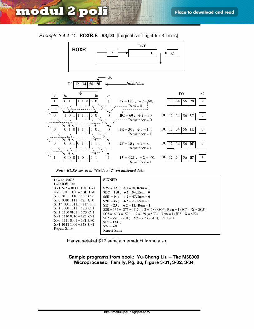
E3165 / UNIT 3 / 55
ASSEMBLY LANGUAGE
Example 3.4.4-11: ROXR.B #3,D0 [Logical shift right for 3 times]
`
Hanya setakat $17 sahaja mematuhi formula ÷÷÷÷ 2, Sample programs from book: Yu-Cheng Liu – The M68000
Microprocessor Family, Pg. 86, Figure 3-31, 3-32, 3-34
Note: ROXR serves as “divide by 2” on unsigned data
12 34 56 D0 78
0 1 1 1 1 0 0 0
b7 b0
1
C
1 0 1 1 1 1 0 0 0
0 1 0 1 1 1 1 0 0
0 0 1 0 1 1 1 1 0
78 = 120 ; ÷ 2 = 60,
Rem = 0
BC = 60 ; ÷ 2 = 30,
Remainder = 0
5E = 30 ; ÷ 2 = 15,
Remainder = 1
2F = 15 ; ÷ 2 = 7,
Remainder = 1
.B
Initial data
12 34 56
D0
78
12 34 56 D0 3C
12 34 56 D0 1E
12 34 56 D0 0F
?
C
0
0
0
0 0 0 1 0 1 1 1 1 17 = -121 ; ÷ 2 = -60,
Remainder = 1
12 34 56 D0 87 1
D0=12345678
LSR.B #?, D0
X=1 $78 = 0111 1000 C=1
X=0 1011 1100 = $BC C=0
X=0 0101 1110 = $5E C=0
X=0 0010 1111 = $2F C=0
X=1* 0001 0111 = $17 C=1
X=1 1000 1011 = $8B C=1
X=1 1100 0101 = $C5 C=1
X=1 1110 0010 = $E2 C=1
X=0 1111 0001 = $F1 C=0
X=1 0111 1000 = $78 C=1
Repeat-Same
SIGNED
$78 = 120 ; ÷÷÷÷ 2 = 60, Rem = 0
$BC = 188 ; ÷÷÷÷ 2 = 94, Rem = 0
$5E = 94 ; ÷÷÷÷ 2 = 47, Rem = 0
$2F = 47 ; ÷÷÷÷ 2 = 23, Rem = 1
$17 = 23 ; ÷÷÷÷ 2 = 11, Rem = 1
$8B = 139 = -$75 = -117; ÷ 2 = -58 (=$C6), Rem = 1 ($C6 - *X = $C5)
$C5 = -$3B = -59 ; ÷ 2 = -29 (= $E3), Rem = 1 ($E3 – X = $E2)
$E2 = -$1E = -30 ; ÷ 2 = -15 (= $F1), Rem = 0
$F1 = 120 ;
$78 = 60
Repeat-Same
C
DST ROXR
X
1
0
0
0
1
X
http://modul2poli.blogspot.com/
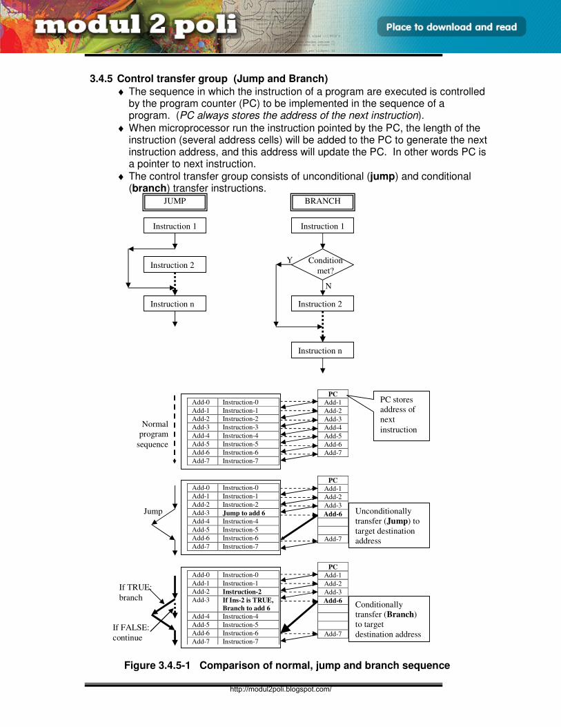
E3165 / UNIT 3 / 56
ASSEMBLY LANGUAGE
3.4.5 Control transfer group (Jump and Branch)
♦ The sequence in which the instruction of a program are executed is controlled by the program counter (PC) to be implemented in the sequence of a program. (PC always stores the address of the next instruction).
♦ When microprocessor run the instruction pointed by the PC, the length of the instruction (several address cells) will be added to the PC to generate the next instruction address, and this address will update the PC. In other words PC is a pointer to next instruction.
♦ The control transfer group consists of unconditional (jump) and conditional (branch) transfer instructions.
Figure 3.4.5-1 Comparison of normal, jump and branch sequence
Add-0 Instruction-0
Add-1 Instruction-1
Add-2 Instruction-2
Add-3 Jump to add 6
Add-4 Instruction-4
Add-5 Instruction-5
Add-6 Instruction-6
Add-7 Instruction-7
Add-0 Instruction-0
Add-1 Instruction-1
Add-2 Instruction-2
Add-3 If Ins-2 is TRUE,
Branch to add 6
Add-4 Instruction-4
Add-5 Instruction-5
Add-6 Instruction-6
Add-7 Instruction-7
Unconditionally
transfer (Jump) to
target destination
address
Conditionally
transfer (Branch)
to target
destination address
Normal
program
sequence
Add-0 Instruction-0
Add-1 Instruction-1
Add-2 Instruction-2
Add-3 Instruction-3
Add-4 Instruction-4
Add-5 Instruction-5
Add-6 Instruction-6
Add-7 Instruction-7
PC
Add-1
Add-2
Add-3
Add-4
Add-5
Add-6
Add-7
PC
Add-1
Add-2
Add-3
Add-6
Add-7
PC
Add-1
Add-2
Add-3
Add-6
Add-7
PC stores
address of
next
instruction
Jump
If TRUE:
branch
If FALSE:
continue
Instruction 1
Instruction 2
Instruction n
JUMP
Instruction 1
Instruction 2
Instruction n
BRANCH
Condition
met?
Y
N
http://modul2poli.blogspot.com/
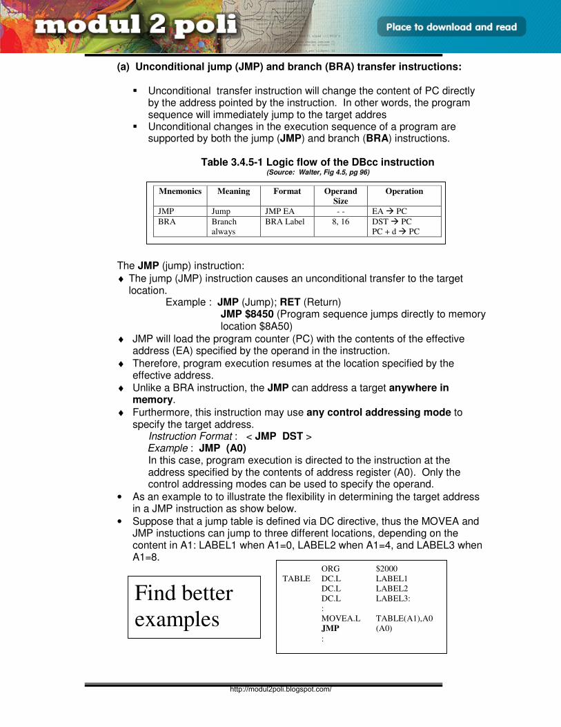
E3165 / UNIT 3 / 57
ASSEMBLY LANGUAGE
(a) Unconditional jump (JMP) and branch (BRA) transfer instructions:
Unconditional transfer instruction will change the content of PC directly by the address pointed by the instruction. In other words, the program sequence will immediately jump to the target addres
Unconditional changes in the execution sequence of a program are supported by both the jump (JMP) and branch (BRA) instructions.
Table 3.4.5-1 Logic flow of the DBcc instruction
(Source: Walter, Fig 4.5, pg 96)
The JMP (jump) instruction:
♦ The jump (JMP) instruction causes an unconditional transfer to the target location.
Example : JMP (Jump); RET (Return) JMP $8450 (Program sequence jumps directly to memory location $8A50)
♦ JMP will load the program counter (PC) with the contents of the effective address (EA) specified by the operand in the instruction.
♦ Therefore, program execution resumes at the location specified by the effective address.
♦ Unlike a BRA instruction, the JMP can address a target anywhere in memory.
♦ Furthermore, this instruction may use any control addressing mode to specify the target address.
Instruction Format : < JMP DST > Example : JMP (A0) In this case, program execution is directed to the instruction at the address specified by the contents of address register (A0). Only the control addressing modes can be used to specify the operand.
• As an example to to illustrate the flexibility in determining the target address in a JMP instruction as show below.
• Suppose that a jump table is defined via DC directive, thus the MOVEA and JMP instuctions can jump to three different locations, depending on the content in A1: LABEL1 when A1=0, LABEL2 when A1=4, and LABEL3 when A1=8.
Mnemonics Meaning Format Operand
Size
Operation
JMP Jump JMP EA - - EA PC
BRA Branch
always
BRA Label 8, 16 DST PC
PC + d PC
ORG $2000
TABLE DC.L LABEL1
DC.L LABEL2
DC.L LABEL3:
:
MOVEA.L TABLE(A1),A0
JMP (A0)
:
Find better
examples
http://modul2poli.blogspot.com/

E3165 / UNIT 3 / 58
ASSEMBLY LANGUAGE
The BRA (branch always) instruction:
♦ BRA differ from JMP in the manner by which the address of the next instruction to be executed is encoded.
♦ In JMP, this address is specified directly by an EA operand, this permits it to reside in a data register or a storage location memory.
♦ In BRA, the difference between the address of the instruction and that of the BRA instruction (displacement) is encoded following the opcode.
♦ Thus, for the BRA instruction the microprocessor computes the next address by adding the displacement to the current value in PC.
♦ The programmer does not normally specify the displacement in the branch instruction. Instead, a label is written in the program to identify the branch to location.
♦ For example: BRA START (displacement in word) This instruction will cause a transfer of program control to the instruction in the
program with the label START. It is the duty of the assembler program to compute the actual displacement and encode it into the instruction.
♦ BRA START has a displacement encoded as a 16-bit word. If displacement must be encoded as a byte, the instruction should be written as:
BRA.S START (displacement in byte)
Figure 3.4.5-1 Sample program for Branch and Jump instruction
Rujuk Pg: 144 (DT502 CM) Sample program with loops (BRA).
Sample program with branch instructions:
MOVE.W AA,D0
CMP.W BB,D0
BGT.S CHECKB
TST.W D0
BGE.S INCA
BRA.S ZEROA
INCA ADDQ.W #1,AA
BRA.S NEXT
CHECKB CMPI.W #-5,BB
BLE.S ZEROA
SUBQ.W #1,AA
BRA.S NEXT
ZEROA CLR.W AA
NEXT :
:
Sample program with Jump instructions:
BRTBL DC.L LABEL1 ;Action1
DC.L LABEL2 ;Action1
:
MOVEA.L #BRTBL,A0
MOVEA.L 0(A0,D7.W),A1
JMP (A1)
SKIP BRA NEXT
:
NEXT :
:
http://modul2poli.blogspot.com/
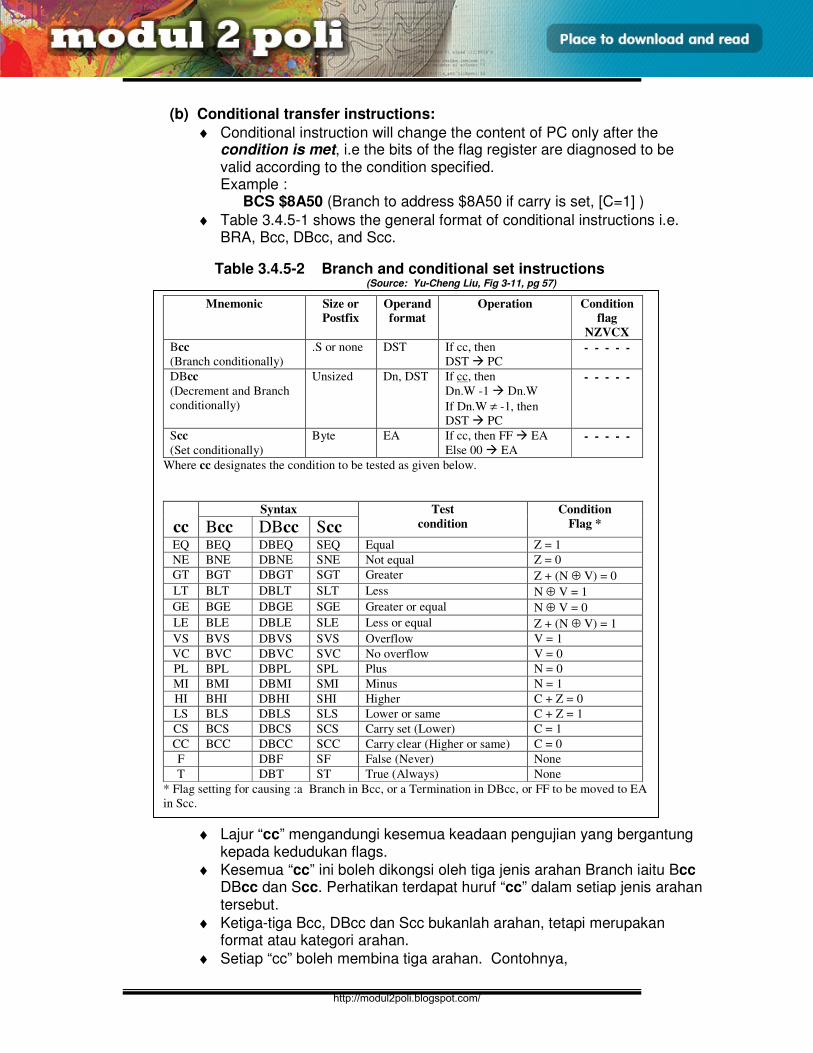
E3165 / UNIT 3 / 59
ASSEMBLY LANGUAGE
(b) Conditional transfer instructions:
♦ Conditional instruction will change the content of PC only after the condition is met, i.e the bits of the flag register are diagnosed to be valid according to the condition specified. Example :
BCS $8A50 (Branch to address $8A50 if carry is set, [C=1] )
♦ Table 3.4.5-1 shows the general format of conditional instructions i.e. BRA, Bcc, DBcc, and Scc.
Table 3.4.5-2 Branch and conditional set instructions (Source: Yu-Cheng Liu, Fig 3-11, pg 57)
♦ Lajur “cc” mengandungi kesemua keadaan pengujian yang bergantung kepada kedudukan flags.
♦ Kesemua “cc” ini boleh dikongsi oleh tiga jenis arahan Branch iaitu Bcc DBcc dan Scc. Perhatikan terdapat huruf “cc” dalam setiap jenis arahan tersebut.
♦ Ketiga-tiga Bcc, DBcc dan Scc bukanlah arahan, tetapi merupakan format atau kategori arahan.
♦ Setiap “cc” boleh membina tiga arahan. Contohnya,
Mnemonic Size or
Postfix
Operand
format
Operation Condition
flag
NZVCX
Bcc
(Branch conditionally)
.S or none DST If cc, then
DST PC - - - - -
DBcc
(Decrement and Branch
conditionally)
Unsized Dn, DST If cc, then
Dn.W -1 Dn.W
If Dn.W ≠ -1, then
DST PC
- - - - -
Scc
(Set conditionally)
Byte EA If cc, then FF EA
Else 00 EA - - - - -
Where cc designates the condition to be tested as given below.
cc Syntax Test
condition
Condition
Flag * Bcc DBcc Scc EQ BEQ DBEQ SEQ Equal Z = 1
NE BNE DBNE SNE Not equal Z = 0
GT BGT DBGT SGT Greater Z + (N ⊕ V) = 0
LT BLT DBLT SLT Less N ⊕ V = 1
GE BGE DBGE SGE Greater or equal N ⊕ V = 0
LE BLE DBLE SLE Less or equal Z + (N ⊕ V) = 1
VS BVS DBVS SVS Overflow V = 1
VC BVC DBVC SVC No overflow V = 0
PL BPL DBPL SPL Plus N = 0
MI BMI DBMI SMI Minus N = 1
HI BHI DBHI SHI Higher C + Z = 0
LS BLS DBLS SLS Lower or same C + Z = 1
CS BCS DBCS SCS Carry set (Lower) C = 1
CC BCC DBCC SCC Carry clear (Higher or same) C = 0
F DBF SF False (Never) None
T DBT ST True (Always) None
* Flag setting for causing :a Branch in Bcc, or a Termination in DBcc, or FF to be moved to EA
in Scc.
http://modul2poli.blogspot.com/
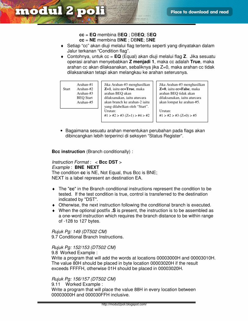
E3165 / UNIT 3 / 60
ASSEMBLY LANGUAGE
cc = EQ membina BEQ ; DBEQ; SEQ cc = NE membina BNE ; DBNE; SNE
♦ Setiap “cc” akan diuji melalui flag tertentu seperti yang dinyatakan dalam Jalur terkanan “Condition flag”.
♦ Contohnya, untuk cc = EQ (Equal) akan diuji melalui flag Z. Jika sesuatu operasi arahan menyebabkan Z menjadi 1, maka cc adalah True, maka arahan cc akan dilaksanakan, sebaliknya jika Z=0, maka arahan cc tidak dilaksanakan tetapi akan melangkau ke arahan seterusnya.
• Bagaimana sesuatu arahan menentukan perubahan pada flags akan dibincangkan lebih terperinci di seksyen “Status Register”.
Bcc instruction (Branch conditionally) :
Instruction Format : < Bcc DST > Example : BNE NEXT The condition cc is NE, Not Equal, thus Bcc is BNE; NEXT is a label represent an destination EA.
♦ The "cc" in the Branch conditional instructions represent the condition to be tested. If the test condition is true, control is transferred to the destination indicated by "DST".
♦ Otherwise, the next instruction following the conditional branch is executed.
♦ When the optional postfix .S is present, the instruction is to be assembled as a one-word instruction which requires the branch distance to be within range of -128 to 127 bytes.
Rujuk Pg: 149 (DT502 CM) 9.7 Conditional Branch Instructions. Rujuk Pg: 152/153 (DT502 CM) 9.8 Worked Example : Write a program that will add the words at locations 00003000H and 00003010H. The value 80H should be placed in byte location 00003020H if the result exceeds FFFFH, otherwise 01H should be placed in 00003020H. Rujuk Pg: 156/157 (DT502 CM) 9.11 Worked Example : Write a program that will place the value 88H in every location between 00003000H and 000030FFH inclusive.
Arahan-#1
Start Arahan-#2
Arahan-#3
BEQ Start
Arahan-#5
Jika Arahan-#3 menghasilkan
Z=1, iaitu cc=True, maka
arahan BEQ akan
dilaksanakan, iaitu aturcara
akan branch ke arahan-2 iaitu
yang dilabelkan oleh “Start”.
Urutan:
#1 > #2 > #3 (Z=1) > #4 > #2
Jika Arahan-#3 menghasilkan
Z=0, iaitu cc=False, maka
arahan BEQ tidak akan
dilaksanakan, iaitu aturcara
akan lompat ke arahan-#5.
Urutan:
#1 > #2 > #3 (Z=0) > #5
http://modul2poli.blogspot.com/
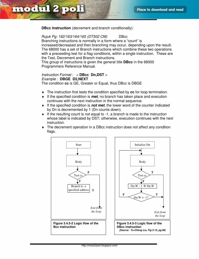
E3165 / UNIT 3 / 61
ASSEMBLY LANGUAGE
DBcc instruction (decrement and branch conditionally): Rujuk Pg: 162/163/164/165 (DT502 CM) DBcc Branching instructions is normally in a form where a “count” is increased/decreased and then branching may occur, depending upon the result. The 68000 has a set of Branch instructions which combine these two operations with a preceeding test for a flag conditions, within a single instruction. These are the Test, Decrement and Branch instructions. This group of instructions is given the general title DBcc in the 68000 Programmers Reference Manual. Instruction Format : < DBcc Dn,DST > Example : DBGE D2,NEXT The condition cc is GE, Greater or Equal, thus DBcc is DBGE
♦ The instruction first tests the condition specified by cc for loop termination.
♦ If the specified condition is met, no branch has taken place and execution continues with the next instruction in the normal sequence.
♦ If the specified condition is not met, the lower word of the counter indicated by Dn is decremented by 1 (Dn counts down).
♦ If the resulting count is not equal to -1, a branch is made to the instruction whose label is indicated by DST; otherwise, execution continues with the next instruction.
♦ The decrement operation in a DBcc instruction does not affect any condition flags.
Initialize Dn
Body
Test cc
Dn.W - 1 Dn.W
Dn.W = -1?
T
T
F
F
Exit from
the loop
Figure 3.4.5-3 Logic flow of the DBcc instruction
(Source: Yu-Cheng Liu, Fig 3-13, pg 60)
Start
Body
Test cc
Branch to a
spesified address
F
T
T
Exit from
the loop
Figure 3.4.5-2 Logic flow of the Bcc instruction
http://modul2poli.blogspot.com/
E3165 / UNIT 3 / 62
ASSEMBLY LANGUAGE
Scc instruction (set conditionally): Instuction Format : < Scc DST > Example : SGE FLAG The condition cc is GE, Greater or Equal, thus Scc is SGE
♦ Scc instruction tests the condition specified by the cc field, as does a Bcc or DBcc instruction.
♦ Unlike the Bcc and DBcc, the test result in an Scc instruction does not cause a branch.
♦ Instead, it is used to set the destination operand either to FF (if the condition is met); or to 00 (if the condition is not met).
♦ The destination operand, which is a byte, can be specified by any data alterable addressing mode.
Sample Program: MOVE.W XX,D1 CMP.W YY,D1 SGE FLAG ; if XX >= YY, FLAG = $FF (is set).
The Bit Test Instruction (BTEST) This instruction can be used to test the state of any single bit within a register or memory location. If the specified bit is at logic 0, the zero flag is set. The register or memory location to be tested can be either 8-bit or 32-bit but not 16-bit. Bits are numbered from 0 on the right thus:
Example: btst.l #25,d1 Rujuk Pg: 181-185 (DT502 CM) Sample program
Rujuk Pg: 186 (DT502 CM) Test Bit and Set Instruction (bset) This instruction tests the state of any given bit within a register or memory location and conditions the Zero flag accordingly (i.e. if bits is 0 then Zero flag is set). This bit is then also set.
Example: bset.l #14,d0 Rujuk Pg: 186 (DT502 CM) Test Bit and Clear Instruction (bclr) This instruction is similar to bset, except that the specified bit is cleared after testing and Zero flag conditioning.
Example: bclr.l #22,d1 Rujuk Pg: 187 (DT502 CM) Test Bit and Change Instruction (bchg) Again, this instruction is similar to bset, except that the specified bit is inverted (i.e. takes the opposite value) after testing and Zero flag conditioning.
Example: bchg.l #27,d2 Rujuk Pg: 188 (DT502 CM) The Negative flag Every negative number in 2’s complement notation has its most significant bit at 1. The Negative flag (N-flag) is set when the most significant bit of a result is 1. This can therefore be used to identify negative results.
Example: bmi #$00001200 Example: bpl 1stwrd
http://modul2poli.blogspot.com/
E3165 / UNIT 3 / 63
ASSEMBLY LANGUAGE
(c) Other control transfer instructions:
♦ The NOP (no operation) instruction has no effect on program execution. This instruction provides a location to be branched to form other places in the program.
♦ In most subroutine perform delay, NOP is used to offest the fraction to produce a precise timing.
♦ The STOP instruction is a priviledged instruction whose operand must be immediate. In the supervisor mode, this instruction loads the immediate word into the status register and then stops.
http://modul2poli.blogspot.com/
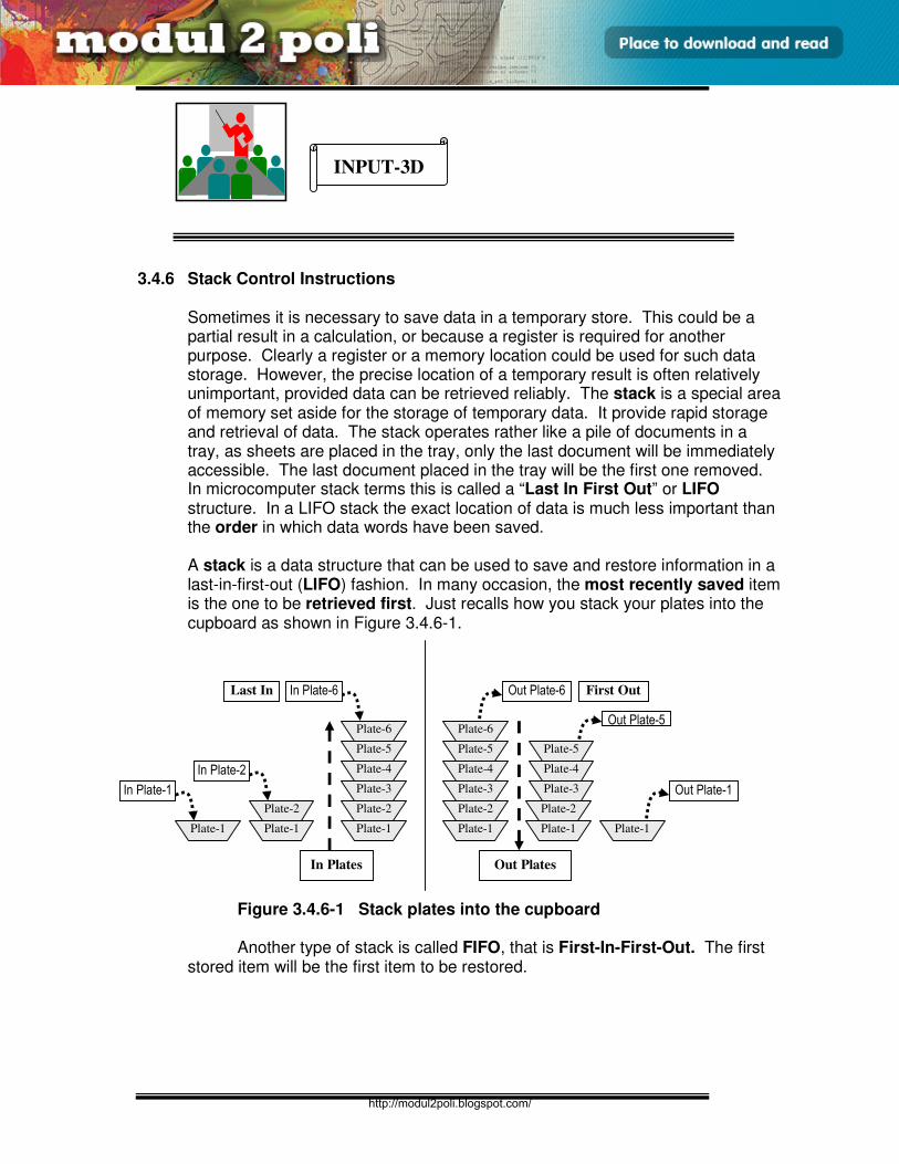
E3165 / UNIT 3 / 64
ASSEMBLY LANGUAGE
3.4.6 Stack Control Instructions
Sometimes it is necessary to save data in a temporary store. This could be a partial result in a calculation, or because a register is required for another purpose. Clearly a register or a memory location could be used for such data storage. However, the precise location of a temporary result is often relatively unimportant, provided data can be retrieved reliably. The stack is a special area of memory set aside for the storage of temporary data. It provide rapid storage and retrieval of data. The stack operates rather like a pile of documents in a tray, as sheets are placed in the tray, only the last document will be immediately accessible. The last document placed in the tray will be the first one removed. In microcomputer stack terms this is called a “Last In First Out” or LIFO structure. In a LIFO stack the exact location of data is much less important than the order in which data words have been saved.
A stack is a data structure that can be used to save and restore information in a last-in-first-out (LIFO) fashion. In many occasion, the most recently saved item is the one to be retrieved first. Just recalls how you stack your plates into the cupboard as shown in Figure 3.4.6-1.
Figure 3.4.6-1 Stack plates into the cupboard Another type of stack is called FIFO, that is First-In-First-Out. The first
stored item will be the first item to be restored.
Plate-1
In Plate-1
Plate-1
In Plate-2
Plate-2
Plate-1
In Plate-6
Plate-2
Plate-3
Plate-4
Plate-5
Plate-6
Plate-1
Out Plate-6
Plate-2
Plate-3
Plate-4
Plate-5
Plate-6
Plate-1
Out Plate-5
Plate-2
Plate-1
Out Plate-1
Last In First Out
In Plates Out Plates
Plate-3
Plate-4
Plate-5
INPUT-3D
http://modul2poli.blogspot.com/
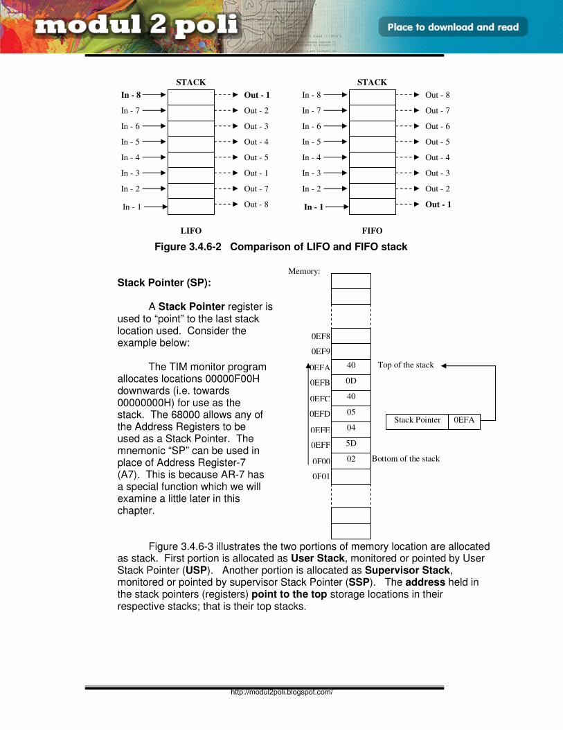
E3165 / UNIT 3 / 65
ASSEMBLY LANGUAGE
Figure 3.4.6-2 Comparison of LIFO and FIFO stack
Stack Pointer (SP): A Stack Pointer register is
used to “point” to the last stack location used. Consider the example below:
The TIM monitor program
allocates locations 00000F00H downwards (i.e. towards 00000000H) for use as the stack. The 68000 allows any of the Address Registers to be used as a Stack Pointer. The mnemonic “SP” can be used in place of Address Register-7 (A7). This is because AR-7 has a special function which we will examine a little later in this chapter.
Figure 3.4.6-3 illustrates the two portions of memory location are allocated
as stack. First portion is allocated as User Stack, monitored or pointed by User Stack Pointer (USP). Another portion is allocated as Supervisor Stack, monitored or pointed by supervisor Stack Pointer (SSP). The address held in the stack pointers (registers) point to the top storage locations in their respective stacks; that is their top stacks.
In - 1
In - 3
In - 4
In - 5
In - 6
In - 7
In - 8
In - 2
Out - 1
Out - 2
Out - 3
Out - 4
Out - 5
Out - 1
Out - 7
Out - 8
STACK
LIFO
In - 1
In - 3
In - 4
In - 5
In - 6
In - 7
In - 8
In - 2
Out - 8
Out - 7
Out - 6
Out - 5
Out - 4
Out - 3
Out - 2
Out - 1
STACK
FIFO
0EF8
0EF9
40
0D
0EFA
0EFB
40
05
0EFC
0EFD
04
5D
0EFE
0EFF
02
0F00
0F01
Memory:
Top of the stack
Bottom of the stack
Stack Pointer 0EFA
http://modul2poli.blogspot.com/
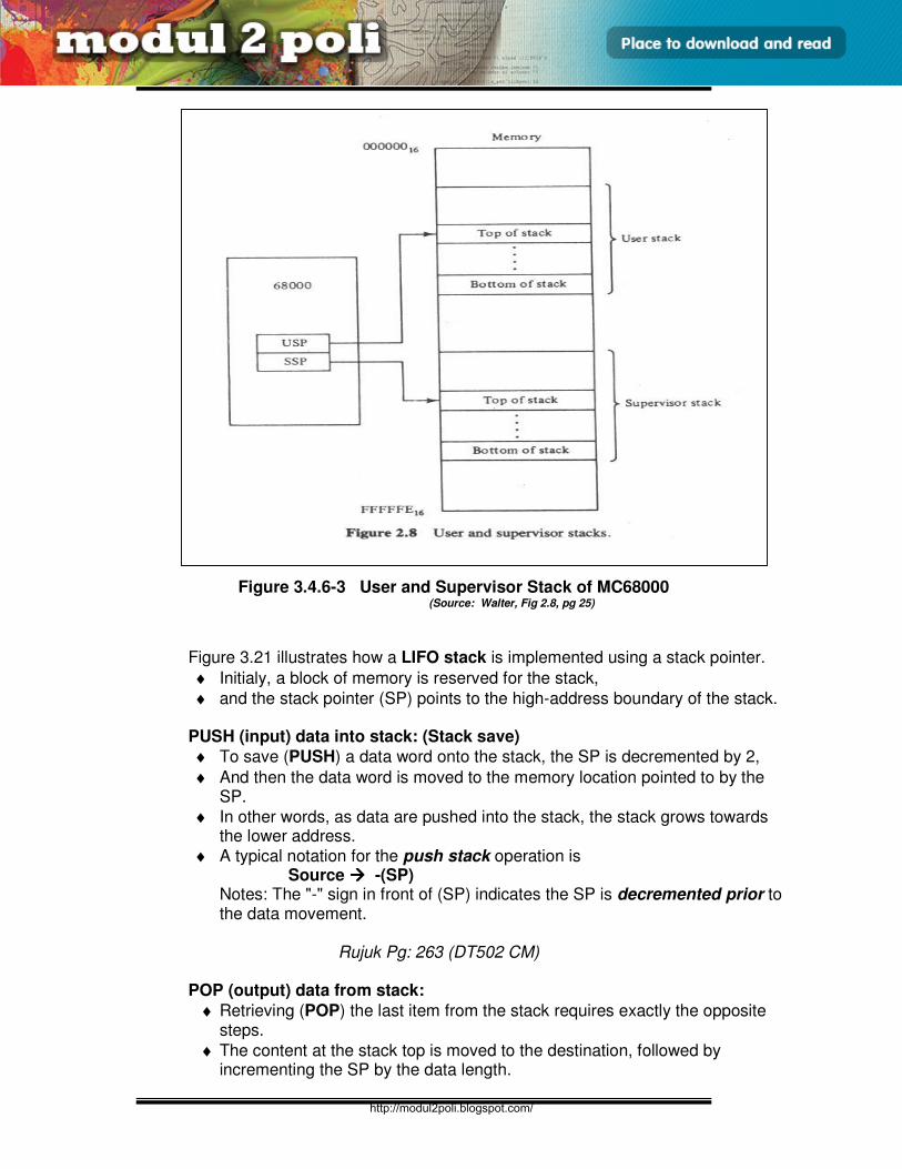
E3165 / UNIT 3 / 66
ASSEMBLY LANGUAGE
Figure 3.4.6-3 User and Supervisor Stack of MC68000
(Source: Walter, Fig 2.8, pg 25)
Figure 3.21 illustrates how a LIFO stack is implemented using a stack pointer.
♦ Initialy, a block of memory is reserved for the stack,
♦ and the stack pointer (SP) points to the high-address boundary of the stack.
PUSH (input) data into stack: (Stack save)
♦ To save (PUSH) a data word onto the stack, the SP is decremented by 2,
♦ And then the data word is moved to the memory location pointed to by the SP.
♦ In other words, as data are pushed into the stack, the stack grows towards the lower address.
♦ A typical notation for the push stack operation is Source -(SP)
Notes: The "-" sign in front of (SP) indicates the SP is decremented prior to the data movement.
Rujuk Pg: 263 (DT502 CM)
POP (output) data from stack:
♦ Retrieving (POP) the last item from the stack requires exactly the opposite steps.
♦ The content at the stack top is moved to the destination, followed by incrementing the SP by the data length.
http://modul2poli.blogspot.com/
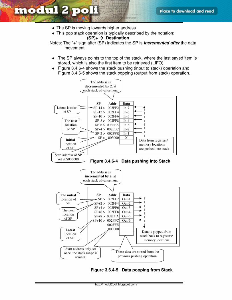
E3165 / UNIT 3 / 67
ASSEMBLY LANGUAGE
♦ The SP is moving towards higher address.
♦ This pop stack operation is typically described by the notation: (SP)+ Destination
Notes: The "+" sign after (SP) indicates the SP is incremented after the data movement.
♦ The SP always points to the top of the stack, where the last saved item is stored, which is also the first item to be retrieved (LIFO).
♦ Figure 3.4.6-4 shows the stack pushing (input to stack) operation and Figure 3.4.6-5 shows the stack popping (output from stack) operation.
Figure 3.6.4-5 Data popping from Stack
SP Addr Data
SP > 002FF2 Out-1
SP+2 > 002FF4 Out-2
SP+4 > 002FF6 Out-3
SP+6 > 002FF8 Out-4
SP+8 > 002FFA Out-5
SP+10 > 002FFC Out-6
002FFE
003000
Data is popped from
stack back to registers/
memory locations
Latest
location
of SP
The next
location
of SP
The address is
incremented by 2, at
each stack advancement
Start address only set
once, the stack range is
remain.
The initial
location of
SP
These data are stored from the
previous pushing operation
SP Addr Data
SP-14 > 002FF2 In-7
SP-12 > 002FF4 In-6
SP-10 > 002FF6 In-5
SP-8 > 002FF8 In-4
SP-6 > 002FFA In-3
SP-4 > 002FFC In-2
SP-2 > 002FFE In-1
SP > 003000 X
Data from registers/
memory locations
are pushed into stack
Initial location
of SP
The next
location
of SP
The address is
decremented by 2, at
each stack advancement
Start address of SP
set at $003000
Latest location of SP
Figure 3.4.6-4 Data pushing into Stack
http://modul2poli.blogspot.com/
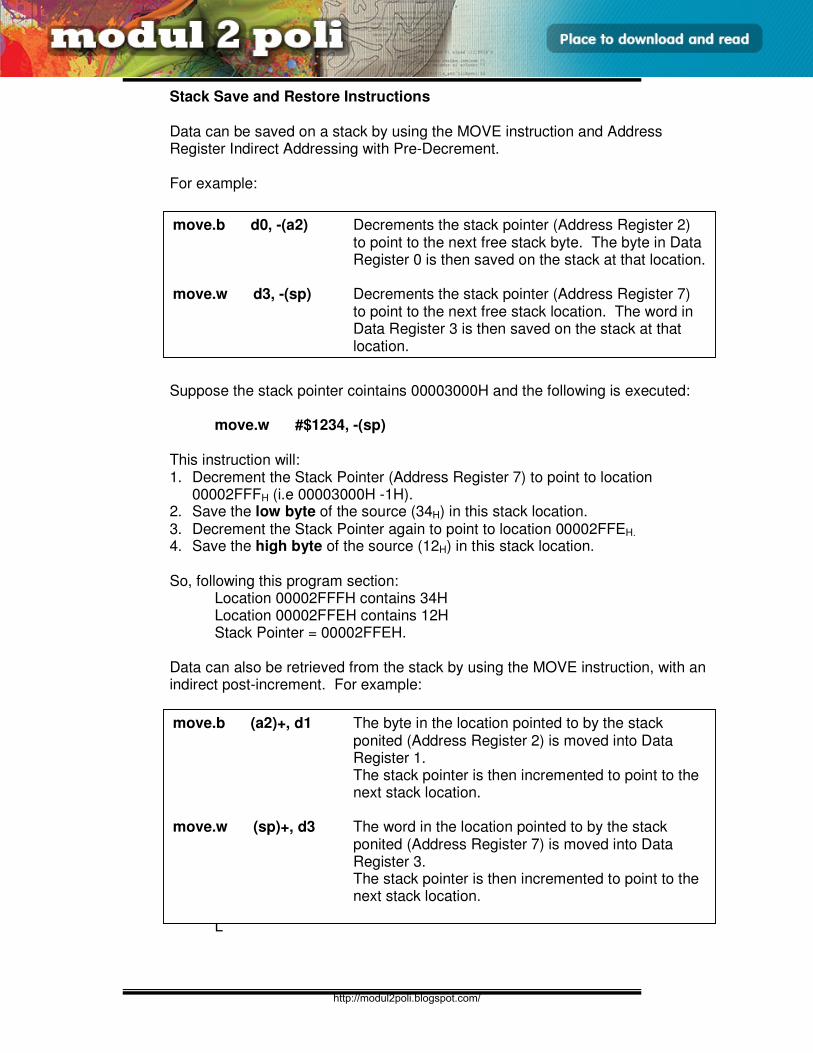
E3165 / UNIT 3 / 68
ASSEMBLY LANGUAGE
Stack Save and Restore Instructions
Data can be saved on a stack by using the MOVE instruction and Address Register Indirect Addressing with Pre-Decrement. For example: Suppose the stack pointer cointains 00003000H and the following is executed:
move.w #$1234, -(sp) This instruction will: 1. Decrement the Stack Pointer (Address Register 7) to point to location
00002FFFH (i.e 00003000H -1H). 2. Save the low byte of the source (34H) in this stack location. 3. Decrement the Stack Pointer again to point to location 00002FFEH. 4. Save the high byte of the source (12H) in this stack location.
So, following this program section:
Location 00002FFFH contains 34H Location 00002FFEH contains 12H Stack Pointer = 00002FFEH.
Data can also be retrieved from the stack by using the MOVE instruction, with an indirect post-increment. For example:
L
move.b d0, -(a2) Decrements the stack pointer (Address Register 2) to point to the next free stack byte. The byte in Data Register 0 is then saved on the stack at that location.
move.w d3, -(sp) Decrements the stack pointer (Address Register 7)
to point to the next free stack location. The word in Data Register 3 is then saved on the stack at that location.
move.b (a2)+, d1 The byte in the location pointed to by the stack ponited (Address Register 2) is moved into Data Register 1. The stack pointer is then incremented to point to the next stack location.
move.w (sp)+, d3 The word in the location pointed to by the stack
ponited (Address Register 7) is moved into Data Register 3. The stack pointer is then incremented to point to the next stack location.
http://modul2poli.blogspot.com/
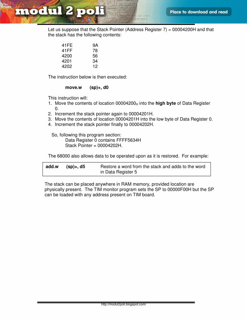
E3165 / UNIT 3 / 69
ASSEMBLY LANGUAGE
Let us suppose that the Stack Pointer (Address Register 7) = 00004200H and that the stack has the following contents:
41FE 9A 41FF 78 4200 56 4201 34 4202 12
The instruction below is then executed:
move.w (sp)+, d0
This instruction will: 1. Move the contents of location 00004200H into the high byte of Data Register
0. 2. Increment the stack pointer again to 00004201H. 3. Move the contents of location 00004201H into the low byte of Data Register 0. 4. Increment the stack pointer finally to 00004202H.
So, following this program section:
Data Register 0 contains FFFF5634H Stack Pointer = 00004202H.
The 68000 also allows data to be operated upon as it is restored. For example:
The stack can be placed anywhere in RAM memory, provided location are physically present. The TIM monitor program sets the SP to 00000F00H but the SP can be loaded with any address present on TIM board.
add.w (sp)+, d5 Restore a word from the stack and adds to the word in Data Register 5
http://modul2poli.blogspot.com/
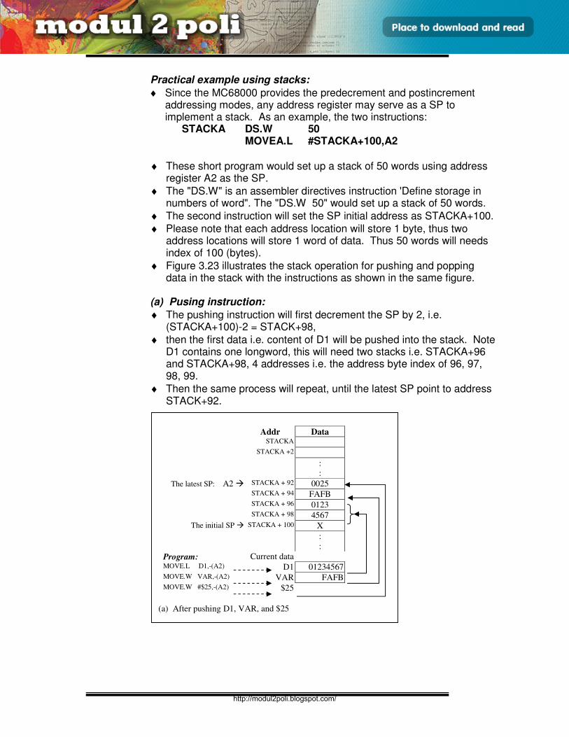
E3165 / UNIT 3 / 70
ASSEMBLY LANGUAGE
Practical example using stacks:
♦ Since the MC68000 provides the predecrement and postincrement addressing modes, any address register may serve as a SP to implement a stack. As an example, the two instructions:
STACKA DS.W 50 MOVEA.L #STACKA+100,A2
♦ These short program would set up a stack of 50 words using address register A2 as the SP.
♦ The "DS.W" is an assembler directives instruction 'Define storage in numbers of word". The "DS.W 50" would set up a stack of 50 words.
♦ The second instruction will set the SP initial address as STACKA+100.
♦ Please note that each address location will store 1 byte, thus two address locations will store 1 word of data. Thus 50 words will needs index of 100 (bytes).
♦ Figure 3.23 illustrates the stack operation for pushing and popping data in the stack with the instructions as shown in the same figure.
(a) Pusing instruction:
♦ The pushing instruction will first decrement the SP by 2, i.e. (STACKA+100)-2 = STACK+98,
♦ then the first data i.e. content of D1 will be pushed into the stack. Note D1 contains one longword, this will need two stacks i.e. STACKA+96 and STACKA+98, 4 addresses i.e. the address byte index of 96, 97, 98, 99.
♦ Then the same process will repeat, until the latest SP point to address STACK+92.
Addr Data
STACKA
STACKA +2
:
:
The latest SP: A2 STACKA + 92 0025
STACKA + 94 FAFB
STACKA + 96 0123
STACKA + 98 4567 The initial SP STACKA + 100 X
:
:
Program: Current data MOVE.L D1,-(A2) D1 01234567 MOVE.W VAR,-(A2) VAR FAFB MOVE.W #$25,-(A2) $25
(a) After pushing D1, VAR, and $25
http://modul2poli.blogspot.com/
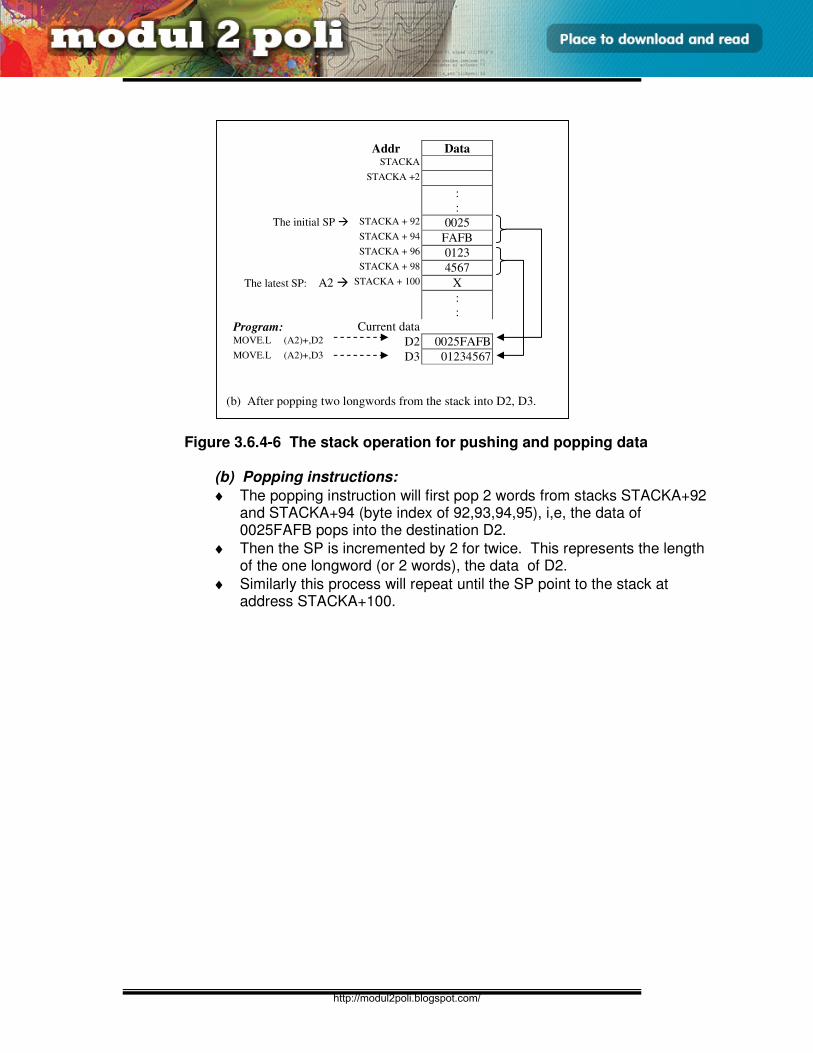
E3165 / UNIT 3 / 71
ASSEMBLY LANGUAGE
Figure 3.6.4-6 The stack operation for pushing and popping data
(b) Popping instructions:
♦ The popping instruction will first pop 2 words from stacks STACKA+92 and STACKA+94 (byte index of 92,93,94,95), i,e, the data of 0025FAFB pops into the destination D2.
♦ Then the SP is incremented by 2 for twice. This represents the length of the one longword (or 2 words), the data of D2.
♦ Similarly this process will repeat until the SP point to the stack at address STACKA+100.
Addr Data
STACKA
STACKA +2
:
: The initial SP STACKA + 92 0025
STACKA + 94 FAFB
STACKA + 96 0123
STACKA + 98 4567
The latest SP: A2 STACKA + 100 X
:
:
Program: Current data MOVE.L (A2)+,D2 D2 0025FAFB MOVE.L (A2)+,D3 D3 01234567
(b) After popping two longwords from the stack into D2, D3.
http://modul2poli.blogspot.com/
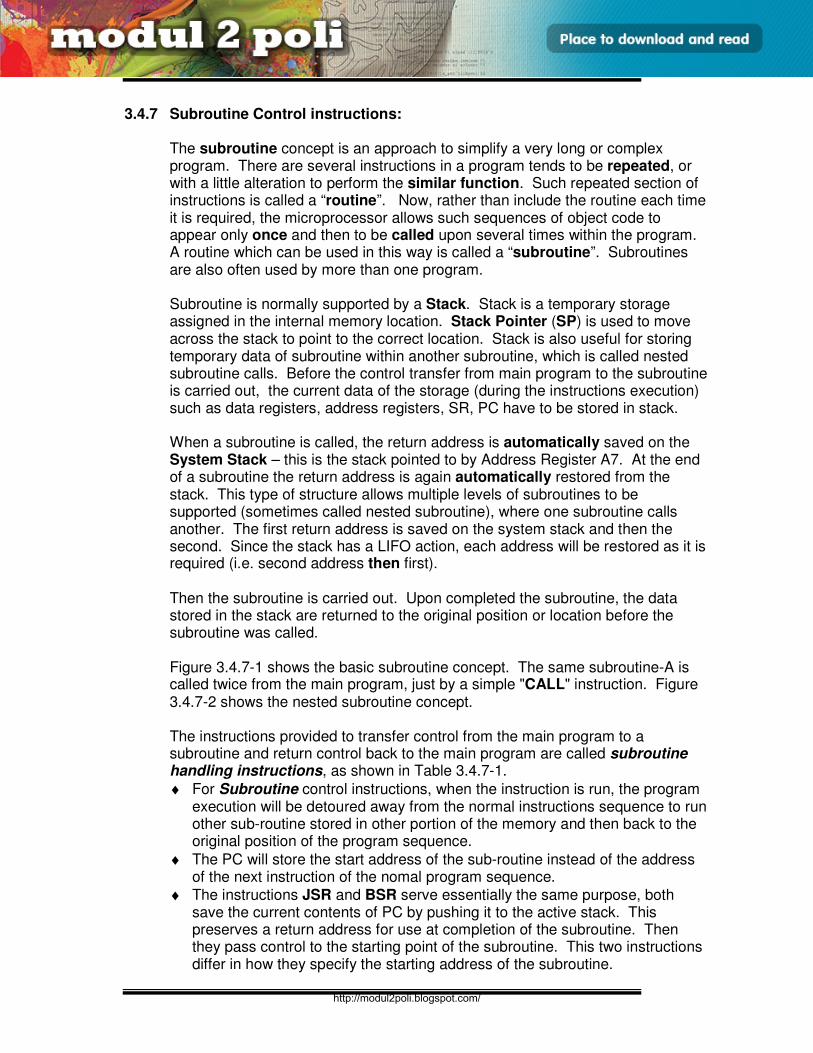
E3165 / UNIT 3 / 72
ASSEMBLY LANGUAGE
3.4.7 Subroutine Control instructions:
The subroutine concept is an approach to simplify a very long or complex program. There are several instructions in a program tends to be repeated, or with a little alteration to perform the similar function. Such repeated section of instructions is called a “routine”. Now, rather than include the routine each time it is required, the microprocessor allows such sequences of object code to appear only once and then to be called upon several times within the program. A routine which can be used in this way is called a “subroutine”. Subroutines are also often used by more than one program. Subroutine is normally supported by a Stack. Stack is a temporary storage assigned in the internal memory location. Stack Pointer (SP) is used to move across the stack to point to the correct location. Stack is also useful for storing temporary data of subroutine within another subroutine, which is called nested subroutine calls. Before the control transfer from main program to the subroutine is carried out, the current data of the storage (during the instructions execution) such as data registers, address registers, SR, PC have to be stored in stack. When a subroutine is called, the return address is automatically saved on the System Stack – this is the stack pointed to by Address Register A7. At the end of a subroutine the return address is again automatically restored from the stack. This type of structure allows multiple levels of subroutines to be supported (sometimes called nested subroutine), where one subroutine calls another. The first return address is saved on the system stack and then the second. Since the stack has a LIFO action, each address will be restored as it is required (i.e. second address then first). Then the subroutine is carried out. Upon completed the subroutine, the data stored in the stack are returned to the original position or location before the subroutine was called. Figure 3.4.7-1 shows the basic subroutine concept. The same subroutine-A is called twice from the main program, just by a simple "CALL" instruction. Figure 3.4.7-2 shows the nested subroutine concept. The instructions provided to transfer control from the main program to a subroutine and return control back to the main program are called subroutine handling instructions, as shown in Table 3.4.7-1.
♦ For Subroutine control instructions, when the instruction is run, the program execution will be detoured away from the normal instructions sequence to run other sub-routine stored in other portion of the memory and then back to the original position of the program sequence.
♦ The PC will store the start address of the sub-routine instead of the address of the next instruction of the nomal program sequence.
♦ The instructions JSR and BSR serve essentially the same purpose, both save the current contents of PC by pushing it to the active stack. This preserves a return address for use at completion of the subroutine. Then they pass control to the starting point of the subroutine. This two instructions differ in how they specify the starting address of the subroutine.
http://modul2poli.blogspot.com/
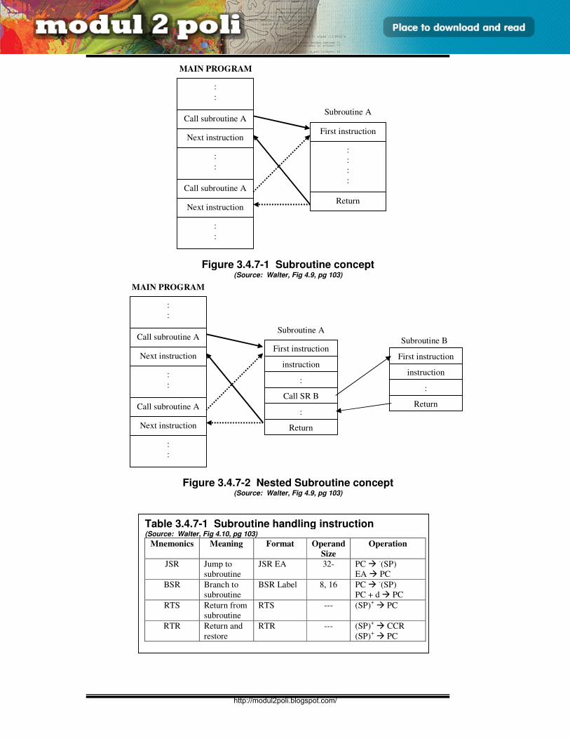
E3165 / UNIT 3 / 73
ASSEMBLY LANGUAGE
Table 3.4.7-1 Subroutine handling instruction (Source: Walter, Fig 4.10, pg 103)
Mnemonics Meaning Format Operand
Size
Operation
JSR Jump to
subroutine
JSR EA 32- PC -(SP)
EA PC
BSR Branch to
subroutine
BSR Label 8, 16 PC -(SP)
PC + d PC
RTS Return from
subroutine
RTS --- (SP)+ PC
RTR Return and
restore
RTR --- (SP)+ CCR
(SP)+ PC
Figure 3.4.7-1 Subroutine concept (Source: Walter, Fig 4.9, pg 103)
Figure 3.4.7-2 Nested Subroutine concept (Source: Walter, Fig 4.9, pg 103)
:
:
Call subroutine A
Next instruction
:
:
Call subroutine A
Next instruction
:
:
First instruction
Return
:
:
:
:
Subroutine A
MAIN PROGRAM
:
:
Call subroutine A
Next instruction
:
:
Call subroutine A
Next instruction
:
:
First instruction
Subroutine A
instruction
:
Return
Call SR B
:
First instruction
instruction
:
Return
Subroutine B
MAIN PROGRAM
http://modul2poli.blogspot.com/
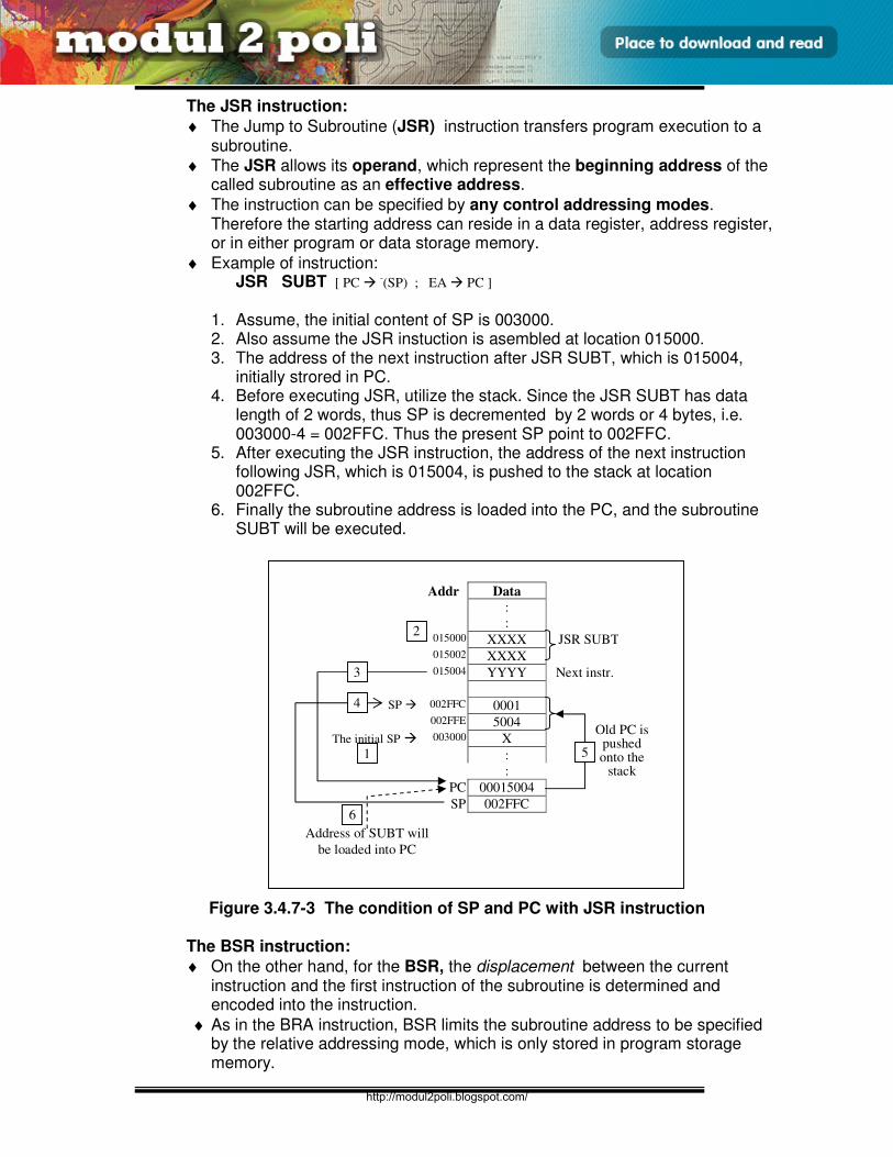
E3165 / UNIT 3 / 74
ASSEMBLY LANGUAGE
The JSR instruction:
♦ The Jump to Subroutine (JSR) instruction transfers program execution to a subroutine.
♦ The JSR allows its operand, which represent the beginning address of the called subroutine as an effective address.
♦ The instruction can be specified by any control addressing modes. Therefore the starting address can reside in a data register, address register, or in either program or data storage memory.
♦ Example of instruction: JSR SUBT [ PC
-(SP) ; EA PC ]
1. Assume, the initial content of SP is 003000. 2. Also assume the JSR instuction is asembled at location 015000. 3. The address of the next instruction after JSR SUBT, which is 015004,
initially strored in PC. 4. Before executing JSR, utilize the stack. Since the JSR SUBT has data
length of 2 words, thus SP is decremented by 2 words or 4 bytes, i.e. 003000-4 = 002FFC. Thus the present SP point to 002FFC.
5. After executing the JSR instruction, the address of the next instruction following JSR, which is 015004, is pushed to the stack at location 002FFC.
6. Finally the subroutine address is loaded into the PC, and the subroutine SUBT will be executed.
Figure 3.4.7-3 The condition of SP and PC with JSR instruction
The BSR instruction:
♦ On the other hand, for the BSR, the displacement between the current instruction and the first instruction of the subroutine is determined and encoded into the instruction.
♦ As in the BRA instruction, BSR limits the subroutine address to be specified by the relative addressing mode, which is only stored in program storage memory.
Addr Data
:
:
015000 XXXX JSR SUBT
015002 XXXX
015004 YYYY Next instr.
SP 002FFC 0001
002FFE 5004
The initial SP 003000 X
:
:
PC 00015004
SP 002FFC
Address of SUBT will
be loaded into PC
Old PC is pushed onto the
stack
6
1
2
3
4
5
http://modul2poli.blogspot.com/
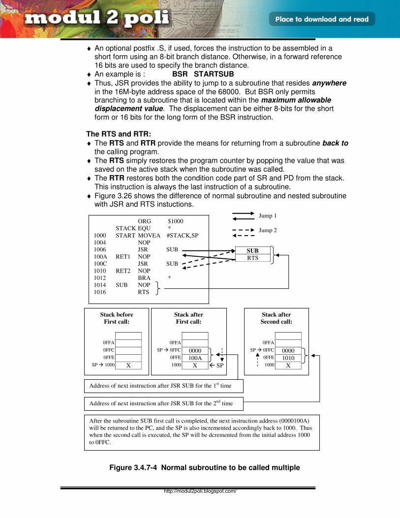
E3165 / UNIT 3 / 75
ASSEMBLY LANGUAGE
♦ An optional postfix .S, if used, forces the instruction to be assembled in a short form using an 8-bit branch distance. Otherwise, in a forward reference 16 bits are used to specify the branch distance.
♦ An example is : BSR STARTSUB
♦ Thus, JSR provides the ability to jump to a subroutine that resides anywhere in the 16M-byte address space of the 68000. But BSR only permits branching to a subroutine that is located within the maximum allowable displacement value. The displacement can be either 8-bits for the short form or 16 bits for the long form of the BSR instruction.
The RTS and RTR:
♦ The RTS and RTR provide the means for returning from a subroutine back to the calling program.
♦ The RTS simply restores the program counter by popping the value that was saved on the active stack when the subroutine was called.
♦ The RTR restores both the condition code part of SR and PD from the stack. This instruction is always the last instruction of a subroutine.
♦ Figure 3.26 shows the difference of normal subroutine and nested subroutine with JSR and RTS instuctions.
Figure 3.4.7-4 Normal subroutine to be called multiple
After the subroutine SUB first call is completed, the next instruction address (0000100A)
will be returned to the PC, and the SP is also incremented accordingly back to 1000. Thus
when the second call is executed, the SP will be dcremented from the initial address 1000
to 0FFC.
ORG $1000
STACK EQU *
1000 START MOVEA #STACK,SP
1004 NOP
1006 JSR SUB
100A RET1 NOP
100C JSR SUB
1010 RET2 NOP
1012 BRA *
1014 SUB NOP
1016 RTS
SUB
RTS
Jump 1
Jump 2
Stack before
First call:
0FFA 0FFC 0FFE
SP 1000 X
Stack after
First call:
0FFA
SP 0FFC 0000 0FFE 100A 1000 X SP
Stack after
Second call:
0FFA
SP 0FFC 0000 0FFE 1010 1000 X
Address of next instruction after JSR SUB for the 2nd
time
Address of next instruction after JSR SUB for the 1st time
http://modul2poli.blogspot.com/
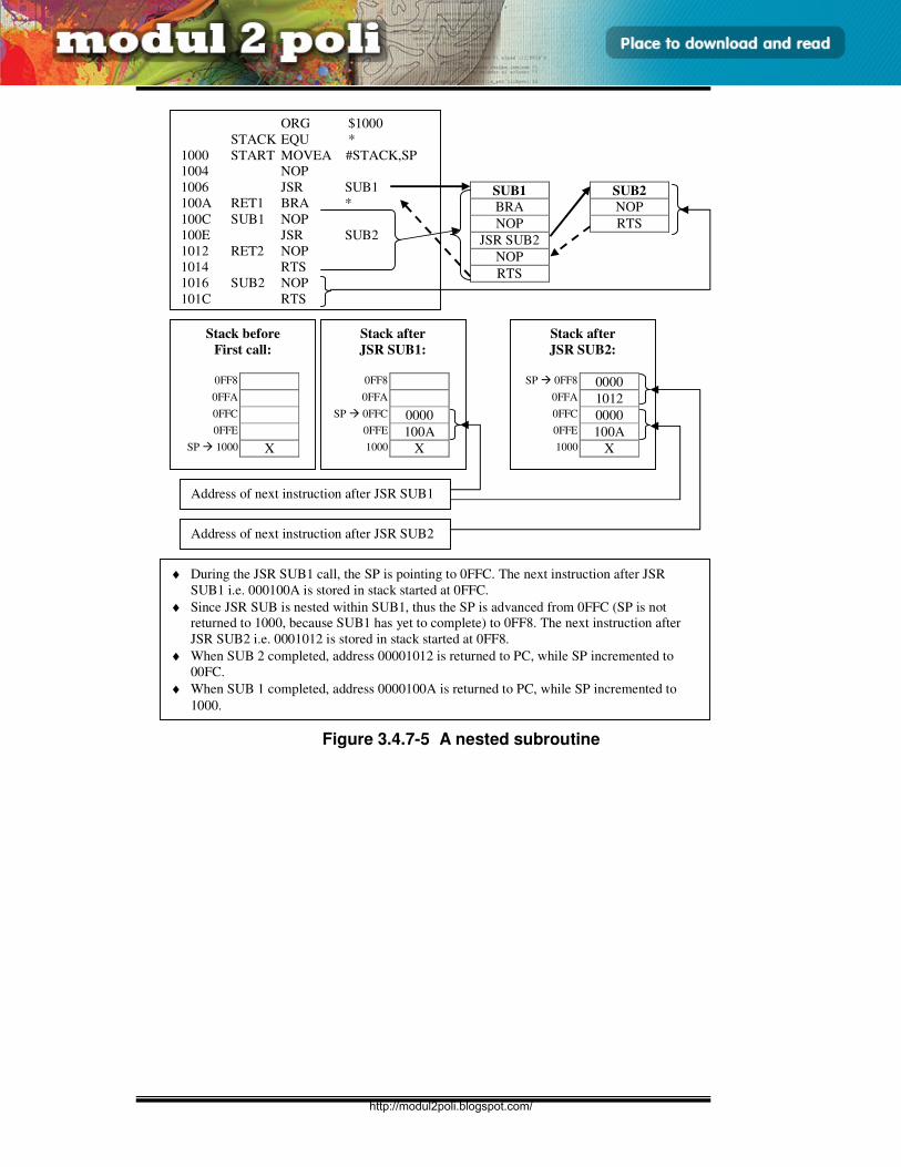
E3165 / UNIT 3 / 76
ASSEMBLY LANGUAGE
Figure 3.4.7-5 A nested subroutine
Stack before
First call:
0FF8 0FFA 0FFC 0FFE
SP 1000 X
Stack after
JSR SUB1:
0FF8 0FFA
SP 0FFC 0000 0FFE 100A 1000 X
Stack after
JSR SUB2: SP 0FF8 0000
0FFA 1012 0FFC 0000 0FFE 100A 1000 X
♦ During the JSR SUB1 call, the SP is pointing to 0FFC. The next instruction after JSR
SUB1 i.e. 000100A is stored in stack started at 0FFC.
♦ Since JSR SUB is nested within SUB1, thus the SP is advanced from 0FFC (SP is not
returned to 1000, because SUB1 has yet to complete) to 0FF8. The next instruction after
JSR SUB2 i.e. 0001012 is stored in stack started at 0FF8.
♦ When SUB 2 completed, address 00001012 is returned to PC, while SP incremented to
00FC.
♦ When SUB 1 completed, address 0000100A is returned to PC, while SP incremented to
1000.
ORG $1000
STACK EQU *
1000 START MOVEA #STACK,SP
1004 NOP
1006 JSR SUB1
100A RET1 BRA *
100C SUB1 NOP
100E JSR SUB2
1012 RET2 NOP
1014 RTS
1016 SUB2 NOP
101C RTS
SUB1
BRA
NOP
JSR SUB2
NOP
RTS
SUB2
NOP
RTS
Address of next instruction after JSR SUB1
Address of next instruction after JSR SUB2
http://modul2poli.blogspot.com/
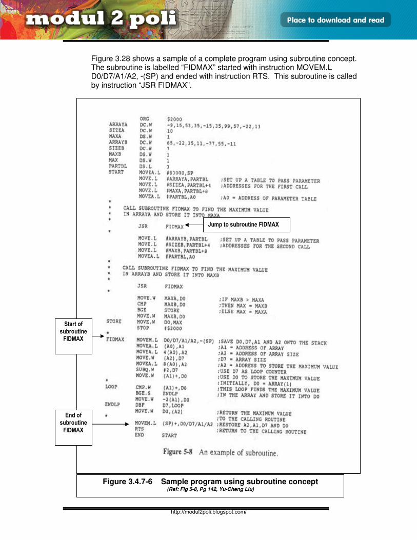
E3165 / UNIT 3 / 77
ASSEMBLY LANGUAGE
Figure 3.28 shows a sample of a complete program using subroutine concept. The subroutine is labelled “FIDMAX” started with instruction MOVEM.L D0/D7/A1/A2, -(SP) and ended with instruction RTS. This subroutine is called by instruction “JSR FIDMAX”.
Figure 3.4.7-6 Sample program using subroutine concept
(Ref: Fig 5-8, Pg 142, Yu-Cheng Liu)
Jump to subroutine FIDMAX
Start of subroutine FIDMAX
End of subroutine
FIDMAX
http://modul2poli.blogspot.com/
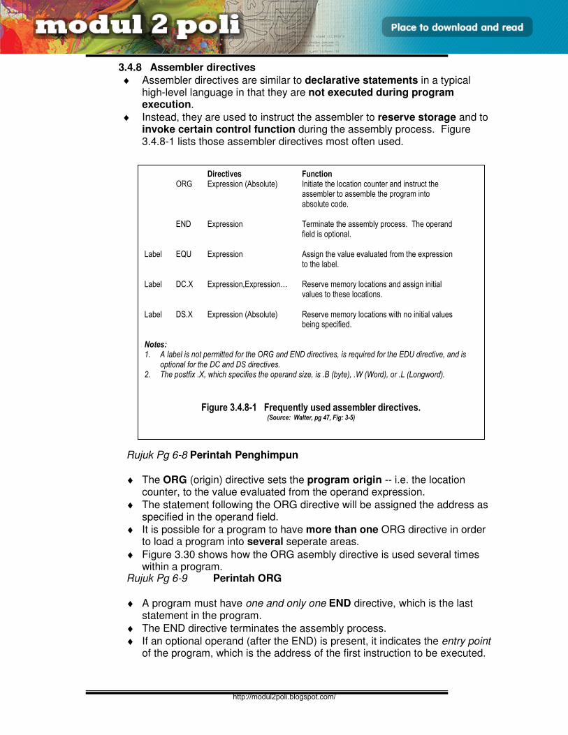
E3165 / UNIT 3 / 78
ASSEMBLY LANGUAGE
3.4.8 Assembler directives
♦ Assembler directives are similar to declarative statements in a typical high-level language in that they are not executed during program execution.
♦ Instead, they are used to instruct the assembler to reserve storage and to invoke certain control function during the assembly process. Figure 3.4.8-1 lists those assembler directives most often used.
Rujuk Pg 6-8 Perintah Penghimpun
♦ The ORG (origin) directive sets the program origin -- i.e. the location counter, to the value evaluated from the operand expression.
♦ The statement following the ORG directive will be assigned the address as specified in the operand field.
♦ It is possible for a program to have more than one ORG directive in order to load a program into several seperate areas.
♦ Figure 3.30 shows how the ORG asembly directive is used several times within a program.
Rujuk Pg 6-9 Perintah ORG
♦ A program must have one and only one END directive, which is the last statement in the program.
♦ The END directive terminates the assembly process.
♦ If an optional operand (after the END) is present, it indicates the entry point of the program, which is the address of the first instruction to be executed.
Directives Function ORG Expression (Absolute) Initiate the location counter and instruct the
assembler to assemble the program into absolute code.
END Expression Terminate the assembly process. The operand
field is optional. Label EQU Expression Assign the value evaluated from the expression
to the label. Label DC.X Expression,Expression… Reserve memory locations and assign initial
values to these locations. Label DS.X Expression (Absolute) Reserve memory locations with no initial values
being specified. Notes: 1. A label is not permitted for the ORG and END directives, is required for the EDU directive, and is
optional for the DC and DS directives. 2. The postfix .X, which specifies the operand size, is .B (byte), .W (Word), or .L (Longword).
Figure 3.4.8-1 Frequently used assembler directives.
(Source: Walter, pg 47, Fig: 3-5)
http://modul2poli.blogspot.com/
E3165 / UNIT 3 / 79
ASSEMBLY LANGUAGE
♦ In case, a main program and several subprograms are assembled independently and then combined into one load module, the main program should be terminated by an END directive with an operand,
♦ Whereas each of the subprograms should be terminated by an END with no operand. This is because the execution of a subprogram is always initiated in a calling program. Consequently, the entry point of the entire program must reside in the main program.
Figure 3.4.8-2 The assembly directive ORG (Source: Yu-Cheng Liu, Section 3-3, pg 47)
Rujuk Pg 6-11 Perintah END
♦ The EQU (equate) directive enables the label to represent the expression in the operand field. Although it is not necessary, this directive provides some conveniences in program coding.
♦ First, the EQU directive allows short names to replace frequently used lengthy expressions, thus reducing actual coding.
♦ Second, it allows meaningful names to represent constants or expressions, thus making a program more readible.
♦ Third, when a frequently used constant or address is replaced with a name, it is easy to change that constant or address in the program if necessary.
Figure 3.4.8-3 The assembly directive EQU (Source: Yu-Cheng Liu, Section 3-3, pg 47) Rujuk Pg 6-8 Perintah EQU
IOREG EQU $8AFE
:
MOVEA.L #IOREG,A1
:
MOVE.B IOREG,D2
:
MOVE.B (A2)+,IOREG
Al llabel IOREG is assigned with address $8AFE
If IOREG EQU $9AAA
All label IOREG is assigned with address $9AAA
ORG $2000
START MOVEA.L #STACK=$600,SP
:
ORG $3000
VAR1 DS.W 5
VAR2 DS.B 8
:
ORG $5000
STACK DS.WL $300
:
Location Contents
:
2000 HHHH
2002 HHHH
:
3000 HHHH
3002 HHHH
:
5000 HHHH
5002 HHHH
:
http://modul2poli.blogspot.com/
E3165 / UNIT 3 / 80
ASSEMBLY LANGUAGE
♦ The operand of DS (define storage) must evaluate to an absolute number that specifies how many bytes, words, or longwords are to be reserved. No initial values will be assigned to the reserved memory block.
♦ The DC (define constant) reserves space and stores the values associated with the operands in the reserved locations. The location of the first element will be aligned to an even address if word or longword is specified.
♦ Both directives require a size postfix .X, where X is B for byte, W for word, or L for longword. An optional label represents the location of the first element of the reserved memory.
♦ Figure 3.32 shows several examples of storage definition directives with the indicated initial contents for the reserved spaces.
Figure 3.4.8-4 Examples of the DC and DS directives
Rujuk Pg 6-10 Perintah DC Rujuk Pg 6-10 Perintah DS
ORG $3000
DC.W $3A78,-17,'AB'
ARY1 DS.W 4
ARY2 DS.B 7
SIZE DC.W ARY2-ARY1
ADDR DC.L ARY2
Location Contents
3000 3A78
3002 FFEF
3004 4142
(ARY1) 3006 ----
3008 ----
300A ----
300C ----
(ARY2) 300E ----
3010 ----
3012 ----
3014 ----
(SIZE) 3016 0008
(ADDR) 3018 0000
301A 300E
Note: - means undefined
Define storage for 4 words
$3006-$300D
Define storage for 7 bytes
$300E-$3015
Define constant "SIZE" with one word of: ARY2 - ARY1 SIZE = ARY2 - ARY1 SIZE = 300E - 3006 =0008 (SIZE) = ($3016) = $0008
ADDR = (ARY2) ADDR = $300E ADDR.L = $0000300E (ADDR) = (3018301B) = $0000300E
$3A78 (.W) $3000/1 -17 = $FFEF (.W) $3002/3 ASCII of : 'A' = $41 ;'B' = $42 'AB' = $4142 (.W) $3004/5
http://modul2poli.blogspot.com/
E3165 / UNIT 3 / 81
ASSEMBLY LANGUAGE
3.5. Flag Register / Status register
In the microprocessor architecture we have known that one of the registers in the MC68000 microprocessor is status register. It is a 16 bits register. Each bit has it own function with some of the bits unused. Figure 3.5-1 illustrates the bits layout of the status register.
Figure 3.5-1 Bits layout of status register
(Source: Yu-Cheng Liu, Fig 2-2, pg 20)
The status register has 16 bits and is divided into the system byte and user byte as shown in Figure 3.5-1. The user byte contains five condition flags. The remaining 3 bits in the user byte are not used and remain zero. The condition flags contain information on the result of the last processor operation. Their flags settings can be tested by conditional branch instructions. The five condition flags are summarized next.
(a) Carry (C)
i). C = 1, carry flag is set if a carry is generated out of the MSB of the result of an instruction operation.
Eg: ADD two 8-bits (word) data.
INPUT-3E
System byte (condition codes register
user byte
15 14 13 12 11 10 9 8 7 6 5 4 3 2 1 0
T 0 S 0 0 I2 I1 I0 0 0 0 X N 7 V C
Trace mode Not used Supervisor state Not used
Interrupt mask Not used
Extand Negative
Zero Overflow
carry
Bits
http://modul2poli.blogspot.com/

E3165 / UNIT 3 / 82
ASSEMBLY LANGUAGE
ii). C = 1 , Borrow = 1 when there is a borrow to MSB Eg : A greater number subtracted from a smaller number. <small> - <Big> = -ve
(b) Overflow (V)
The overflow (V) flag is set when the result exceeds the maxumum number that can be represented in the 2's complement notation for the destination operand size. (i) V = 1; overflow is set when the addition of two positive numbers produces a negative result
[ (+ve) + (+ve) = (-ve) V =1] Eg : 7000 0000 + 4000 0000 = ? From calculator : 7000 0000 + 4000 0000 =B000 0000 V = 1 As we know, the MSB will determine if a number is positive or negative, thus we just analyze the MSD of the 8 hexadecimal digit, as shown follows: Eg : 2000 0000 + 4000 0000 = ? From calculator : 2000 0000 + 4000 0000 = 6000 0000
(+ve) + (+ve) = (+ve) V = 0
MSB: b7 b8 = 1
∴ C = 1
E E
+ 7 0
1 5 E
1 1 1 0 1 1 1 0
+ 0 1 1 1 0 0 0 0
1 0 1 0 1 1 1 1 0
b7
1
b8
1
1
MSB: b8 b7 = 1
∴ C = 1
E E
- F 0
1 F E
1 1 1 0 1 1 1 0
- 1 1 1 1 0 0 0 0
1 1 1 1 1 1 1 1 0
0 2
0 2
0 2 1 2
7… = 0 1 1 1…
↓ MSB = 0
(+ve number)
4… = 0 1 0 0…
↓ MSB = 0
(+ve number)
B… = 1 0 1 1…
↓ MSB = 1
(-ve number)
+ =
Addition operation: (+ve) + (+ve) = (-ve) : abnormal V = 1 (+ve) + (+ve) = (+ve) : normal V = 0
http://modul2poli.blogspot.com/
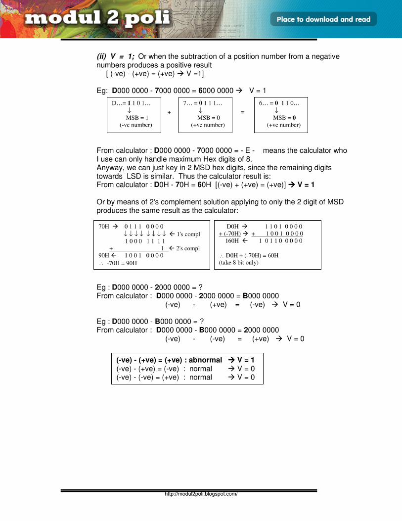
E3165 / UNIT 3 / 83
ASSEMBLY LANGUAGE
(ii) V = 1; Or when the subtraction of a position number from a negative numbers produces a positive result
[ (-ve) - (+ve) = (+ve) V =1] Eg: D000 0000 - 7000 0000 = 6000 0000 V = 1 From calculator : D000 0000 - 7000 0000 = - E - means the calculator who I use can only handle maximum Hex digits of 8. Anyway, we can just key in 2 MSD hex digits, since the remaining digits towards LSD is similar. Thus the calculator result is: From calculator : D0H - 70H = 60H [(-ve) + (+ve) = (+ve)] V = 1 Or by means of 2's complement solution applying to only the 2 digit of MSD produces the same result as the calculator:
Eg : D000 0000 - 2000 0000 = ? From calculator : D000 0000 - 2000 0000 = B000 0000
(-ve) - (+ve) = (-ve) V = 0
Eg : D000 0000 - B000 0000 = ? From calculator : D000 0000 - B000 0000 = 2000 0000
(-ve) - (-ve) = (+ve) V = 0
70H 0 1 1 1 0 0 0 0
↓ ↓ ↓ ↓ ↓ ↓ ↓ ↓ 1's compl
1 0 0 0 1 1 1 1
+ 1 2's compl
90H 1 0 0 1 0 0 0 0
∴ -70H = 90H
D0H 1 1 0 1 0 0 0 0
+ (-70H) + 1 0 0 1 0 0 0 0
160H 1 0 1 1 0 0 0 0 0
∴ D0H + (-70H) = 60H
(take 8 bit only)
D…= 1 1 0 1…
↓ MSB = 1
(-ve number)
7… = 0 1 1 1…
↓ MSB = 0
(+ve number)
6… = 0 1 1 0…
↓ MSB = 0
(+ve number)
+ =
(-ve) - (+ve) = (+ve) : abnormal V = 1 (-ve) - (+ve) = (-ve) : normal V = 0 (-ve) - (-ve) = (+ve) : normal V = 0
http://modul2poli.blogspot.com/
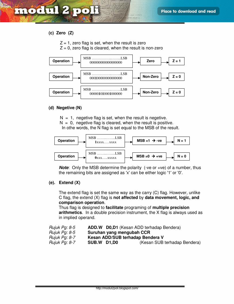
E3165 / UNIT 3 / 84
ASSEMBLY LANGUAGE
(c) Zero (Z)
Z = 1, zero flag is set, when the result is zero Z = 0, zero flag is cleared, when the result is non-zero
(d) Negetive (N) N = 1, negetive flag is set, when the result is negetive. N = 0, negetive flag is cleared, when the result is positive. In othe words, the N flag is set equal to the MSB of the result.
Note: Only the MSB determine the polarity (-ve or +ve) of a number, thus the remaining bits are assigned as 'x' can be either logic '1' or '0'.
(e). Extend (X)
The extend flag is set the same way as the carry (C) flag. However, unlike C flag, the extend (X) flag is not affected by data movement, logic, and comparison operation. Thus flag is designed to facilitate programing of multiple precision arithmetics. In a double precision instrument, the X flag is always used as in implied operand.
Rujuk Pg: 8-5 ADD.W D0,D1 (Kesan ADD terhadap Bendera) Rujuk Pg: 8-5 Suruhan yang mengubah CCR Rujuk Pg: 8-7 Kesan ADD/SUB terhadap Bendera V Rujuk Pg: 8-7 SUB.W D1,D0 (Kesan SUB terhadap Bendera)
Operation MSB ……………..……..LSB
000000000000000000 Zero
Operation MSB ……………..……..LSB
000100000000000000 Non-Zero
Operation MSB ……………..……..LSB
000001010001000000
Z = 1
Z = 0
Z = 0 Non-Zero
Operation MSB ……..……..LSB
1xxxx.….xxxx MSB =1 -ve N = 1
Operation MSB ……..……..LSB
0xxx…..xxxxx MSB =0 +ve N = 0
http://modul2poli.blogspot.com/

E3165 / UNIT 3 / 85
ASSEMBLY LANGUAGE
Contoh:
Jika data awal bagi status register (SR) ialah $A700 dan D2=66778899, apakah data akhir D2
dan SR setelah operasi ADDI.B #$5E,D2 dilaksanakan. Tunjukkan bagaimana setiap bit
bendera (Flag) diperolehi.
ADDI.B #$5E,D2 D2.B=$5E+D2.B=$5E+$99 = ?
5E 0 1 0 1 1 1 1 0
+ 99 + 1 0 0 1 1 0 0 1
F7 1 1 1 1 0 1 1 1
MSB =1, N=1
Bukan
semua bit
= 0,
Z =0
Tiada carry, C=0
15 14 13 12 11 10 9 8 7 6 5 4 3 2 1 0 Bits SR T 0 S 0 0 I2 I1 I0 0 0 0 X N Z V C
Awal A700 1 0 1 0 0 1 1 1 0 0 0 0 0 0 0 0
Akhir A708 1 0 1 0 0 1 1 1 0 0 0 0 1 0 0 0
MSB=0 = +ve
MSB=1 = -ve
MSB=1 = -ve
(<+> + <-> = <-> Normal,
Tidak overflow; V=0
Untuk operasi ADD, X=C=0
Pendaftar SR D2
Awal A700 66778899
Akhir A708 667788F7
1 markah
1 markah
3 markah
http://modul2poli.blogspot.com/
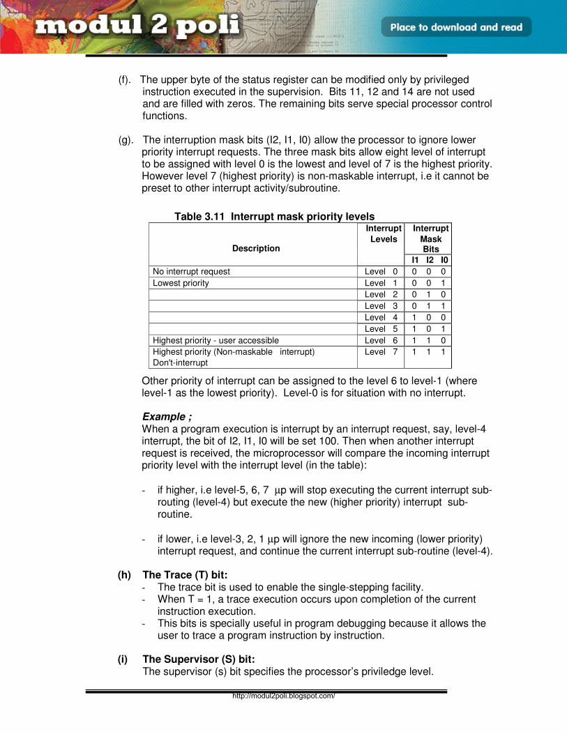
E3165 / UNIT 3 / 86
ASSEMBLY LANGUAGE
(f). The upper byte of the status register can be modified only by privileged
instruction executed in the supervision. Bits 11, 12 and 14 are not used and are filled with zeros. The remaining bits serve special processor control functions.
(g). The interruption mask bits (I2, I1, I0) allow the processor to ignore lower
priority interrupt requests. The three mask bits allow eight level of interrupt to be assigned with level 0 is the lowest and level of 7 is the highest priority. However level 7 (highest priority) is non-maskable interrupt, i.e it cannot be preset to other interrupt activity/subroutine.
Other priority of interrupt can be assigned to the level 6 to level-1 (where
level-1 as the lowest priority). Level-0 is for situation with no interrupt. Example ; When a program execution is interrupt by an interrupt request, say, level-4
interrupt, the bit of I2, I1, I0 will be set 100. Then when another interrupt request is received, the microprocessor will compare the incoming interrupt priority level with the interrupt level (in the table):
- if higher, i.e level-5, 6, 7 µp will stop executing the current interrupt sub-routing (level-4) but execute the new (higher priority) interrupt sub-routine.
- if lower, i.e level-3, 2, 1 µp will ignore the new incoming (lower priority) interrupt request, and continue the current interrupt sub-routine (level-4).
(h) The Trace (T) bit:
- The trace bit is used to enable the single-stepping facility. - When T = 1, a trace execution occurs upon completion of the current
instruction execution. - This bits is specially useful in program debugging because it allows the
user to trace a program instruction by instruction.
(i) The Supervisor (S) bit: The supervisor (s) bit specifies the processor’s priviledge level.
Table 3.11 Interrupt mask priority levels
Description
Interrupt Interrupt
Levels Mask Bits
I1 I2 I0
No interrupt request Level 0 0 0 0
Lowest priority Level 1 0 0 1
Level 2 0 1 0
Level 3 0 1 1
Level 4 1 0 0
Level 5 1 0 1
Highest priority - user accessible Level 6 1 1 0
Highest priority (Non-maskable interrupt) Level 7 1 1 1
Don't-interrupt
http://modul2poli.blogspot.com/
E3165 / UNIT 3 / 87
ASSEMBLY LANGUAGE
If S = 1, the processor is in the supervisor state .
- all instructions can be executed, is typically reversed for the operation system.
If S = 0, the processor is in the user state .
- an attempt to execute a priviledged instruction will cause a trap. - This prevents a user program from changing vital processor
control functions and therefore provides a protection for the system software in a multiprogramming environment.
- After a reset, the processor is initially in the supervisor state, - change from the supervisor state to the user satte can be accomplished
by clearing the S bit. - Since the S bit is not accessible in the user state, a transition back to the
supervisor state can be accomplished only through exeception processing such as traps.
Rujuk Pg:8-2 to 8-4 Daftar CCR
http://modul2poli.blogspot.com/
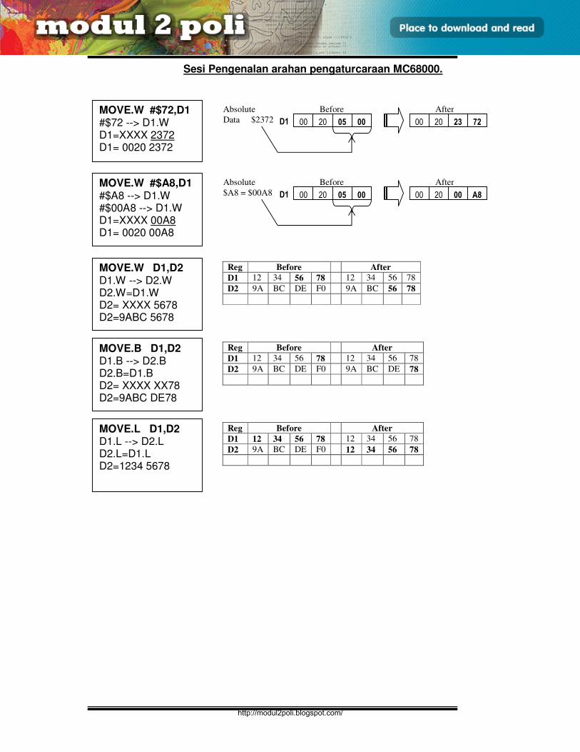
E3165 / UNIT 3 / 88
ASSEMBLY LANGUAGE
Sesi Pengenalan arahan pengaturcaraan MC68000.
MOVE.W #$72,D1 #$72 --> D1.W D1=XXXX 2372 D1= 0020 2372
Before After Absolute
Data $2372 00 20 05 00 D1 00 20 23 72
MOVE.W #$A8,D1 #$A8 --> D1.W #$00A8 --> D1.W D1=XXXX 00A8 D1= 0020 00A8
Before After Absolute
$A8 = $00A8 00 20 05 00 D1 00 20 00 A8
MOVE.W D1,D2 D1.W --> D2.W D2.W=D1.W D2= XXXX 5678 D2=9ABC 5678
Reg Before After
D1 12 34 56 78 12 34 56 78
D2 9A BC DE F0 9A BC 56 78
MOVE.B D1,D2 D1.B --> D2.B D2.B=D1.B D2= XXXX XX78 D2=9ABC DE78
Reg Before After
D1 12 34 56 78 12 34 56 78
D2 9A BC DE F0 9A BC DE 78
MOVE.L D1,D2 D1.L --> D2.L D2.L=D1.L D2=1234 5678
Reg Before After
D1 12 34 56 78 12 34 56 78
D2 9A BC DE F0 12 34 56 78
http://modul2poli.blogspot.com/
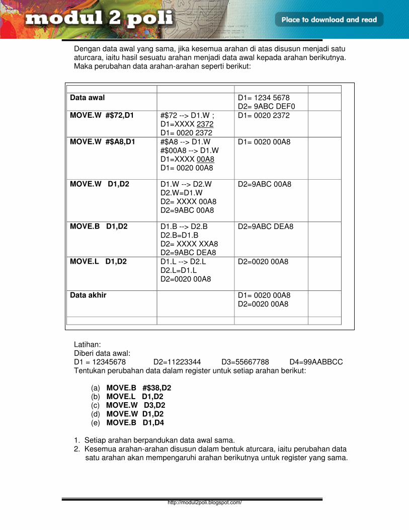
E3165 / UNIT 3 / 89
ASSEMBLY LANGUAGE
Dengan data awal yang sama, jika kesemua arahan di atas disusun menjadi satu aturcara, iaitu hasil sesuatu arahan menjadi data awal kepada arahan berikutnya. Maka perubahan data arahan-arahan seperti berikut: Latihan: Diberi data awal: D1 = 12345678 D2=11223344 D3=55667788 D4=99AABBCC Tentukan perubahan data dalam register untuk setiap arahan berikut:
(a) MOVE.B #$38,D2 (b) MOVE.L D1,D2 (c) MOVE.W D3,D2 (d) MOVE.W D1,D2 (e) MOVE.B D1,D4
1. Setiap arahan berpandukan data awal sama. 2. Kesemua arahan-arahan disusun dalam bentuk aturcara, iaitu perubahan data
satu arahan akan mempengaruhi arahan berikutnya untuk register yang sama.
Data awal D1= 1234 5678 D2= 9ABC DEF0
MOVE.W #$72,D1 #$72 --> D1.W ; D1=XXXX 2372 D1= 0020 2372
D1= 0020 2372
MOVE.W #$A8,D1 #$A8 --> D1.W #$00A8 --> D1.W D1=XXXX 00A8 D1= 0020 00A8
D1= 0020 00A8
MOVE.W D1,D2 D1.W --> D2.W D2.W=D1.W D2= XXXX 00A8 D2=9ABC 00A8
D2=9ABC 00A8
MOVE.B D1,D2 D1.B --> D2.B D2.B=D1.B D2= XXXX XXA8 D2=9ABC DEA8
D2=9ABC DEA8
MOVE.L D1,D2 D1.L --> D2.L D2.L=D1.L D2=0020 00A8
D2=0020 00A8
Data akhir D1= 0020 00A8
D2=0020 00A8
http://modul2poli.blogspot.com/
E3165 / UNIT 3 / 90
ASSEMBLY LANGUAGE
The MC68000 The MC68000 The MC68000 The MC68000
instructions set in instructions set in instructions set in instructions set in
alphabetical orderalphabetical orderalphabetical orderalphabetical order
Source: Source: Source: Source:
YuYuYuYu----Cheng Liu, 1991, The M68000 Microprocessor FamilyCheng Liu, 1991, The M68000 Microprocessor FamilyCheng Liu, 1991, The M68000 Microprocessor FamilyCheng Liu, 1991, The M68000 Microprocessor Family----
Fundamentals of Assembly Language Programming & Fundamentals of Assembly Language Programming & Fundamentals of Assembly Language Programming & Fundamentals of Assembly Language Programming &
Interface DesignInterface DesignInterface DesignInterface Design
Appendix 3-1
http://modul2poli.blogspot.com/
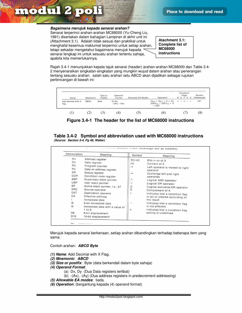
E3165 / UNIT 3 / 91
ASSEMBLY LANGUAGE
Bagaimana merujuk kepada senarai arahan? Senarai terperinci arahan-arahan MC68000 (Yu-Cheng Liu, 1991) disertakan dalam bahagian Lampiran di akhir unit ini (Attachment 3.1). Adalah tidak sesuai dan praktikal untuk menghafal kesemua maklumat terperinci untuk setiap arahan, tetapi sekadar mengetahui bagaimana merujuk kepada senarai lengkap ini untuk sesuatu arahan tertentu sahaja, apabila kita memerlukannya. Rajah 3.4-1 menunjukkan kepala tajuk senarai (header) arahan-arahan MC68000 dan Table 3.4-2 menyenaraikan singkatan-singkatan yang mungkin wujud dalam arahan atau penerangan tentang sesuatu arahan. salah satu arahan iaitu ABCD akan dijadikan sebagai rujukan perbincangan di bawah ini:
Figure 3.4-1 The header for the list of MC68000 instructions
Merujuk kepada senarai berkenaan, setiap arahan dibandingkan terhadap beberapa item yang sama: Contoh arahan: ABCD Byte (1) Name: Add Decimal with X Flag. (2) Mnemonic: ABCD (3) Size or postfix: Byte (data berkendali dalam byte sahaja) (4) Operand Format:
(a) Dx, Dy (Dua Data registers terlibat) (b) -(Ax), -(Ay) (Dua address registers in predecrement addressing)
(5) Allowable EA modes: tiada. (6) Operation: (bergantung kepada (4) operand format)
Atachment 3.1: Complete list of MC68000 instructions
(1) (2) (3) (4) (5) (6) (7) (8)
Table 3.4-2 Symbol and abbreviation used with MC68000 instructions (Source: Section 3-4, Pg 48, Walter)
http://modul2poli.blogspot.com/
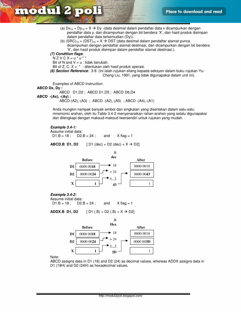
E3165 / UNIT 3 / 92
ASSEMBLY LANGUAGE
(a) Dx10 + Dy10 + X Dy (data desimal dalam pendaftar data x dicampurkan dengan pendaftar data y, dan dicampurkan dengan bit bendera ‘X’, dan hasil produk disimpan dalam pendaftar data terkemudian (Dy)).
(b) (SRC)10 + (DST)10 + X DST (data desimal dalam pendaftar alamat punca dicampurkan dengan pendaftar alamat destinasi, dan dicampurkan dengan bit bendera ‘X’, dan hasil produk disimpan dalam pendaftar alamat destinasi.).
(7) Condition flags: N Z V C X = u * u * * Bit of N and V = u : tidak berubah. Bit of Z, C, X = * : ditentukan oleh hasil produk operasi.
(8) Section Reference: 3-8 (ini ialah rujukan silang kepada seksyen dalam buku rujukan Yu-Cheng Liu, 1991, yang tidak digunapakai dalam unit ini).
Examples of ABCD instruction:
ABCD Dx, Dy : ABCD D1,D2 ; ABCD D1,D5 ; ABCD D6,D4
ABCD -(Ax), -(Ay) : ABCD-(A2),-(A3) ; ABCD -(A2),-(A5) ; ABCD -(A4),-(A1)
Anda mungkin nampak banyak simbol dan singkatan yang disertakan dalam satu-satu mnemonic arahan, oleh itu Table 3.4-2 menyenaraikan rahan-arahan yang selalu digunapakai dan dilengkapi dengan maksud-maksud twersendiri untuk rujukan yang mudah.
Example 3.4-1: Assume initial data: D1.B = 18 ; D2.B = 24 ; and X flag = 1 ABCD.B D1, D2 [ D1 (dec) + D2 (dec) + X D2]
Example 3.4-2: Assume initial data: D1.B = 18 ; D2.B = 24 ; and X flag = 1 ADDX.B D1, D2 [ D1 (.B) + D2 (.B) + X D2]
Note: ABCD assigns data in D1 (18) and D2 (24) as decimal values, whereas ADDX assigns data in D1 (18H) and D2 (24H) as hexadecimal values.
0000 0018
Before
D1
0000 0024 D2
.B
dec
18
+ 24
+ 1
43
0000 0018
After
0000 0043
1 X 1
0000 0018
Before
D1
0000 0024 D2
.B
Hex
18
+ 24
+ 1
3D
0000 0018
After
0000 003D
1 X 1
http://modul2poli.blogspot.com/
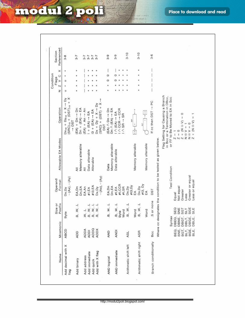
E3165 / UNIT 3 / 93
ASSEMBLY LANGUAGE
http://modul2poli.blogspot.com/
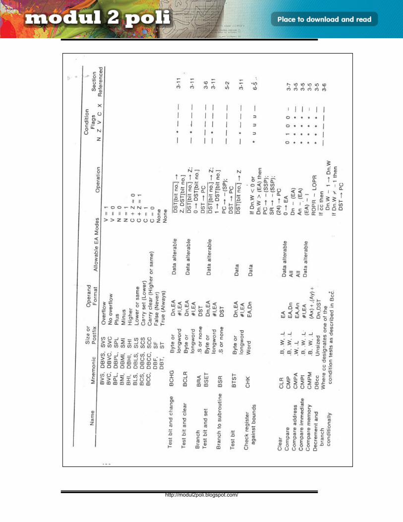
E3165 / UNIT 3 / 94
ASSEMBLY LANGUAGE
http://modul2poli.blogspot.com/
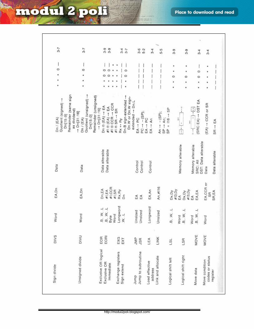
E3165 / UNIT 3 / 95
ASSEMBLY LANGUAGE
http://modul2poli.blogspot.com/
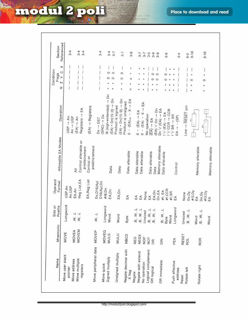
E3165 / UNIT 3 / 96
ASSEMBLY LANGUAGE
http://modul2poli.blogspot.com/
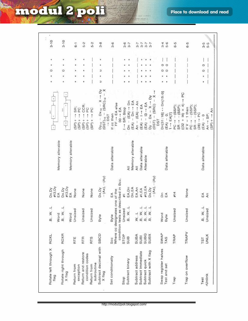
E3165 / UNIT 3 / 97
ASSEMBLY LANGUAGE
http://modul2poli.blogspot.com/
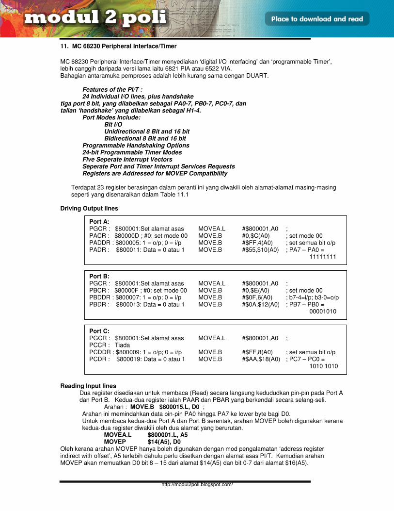
E3165 / UNIT 3 / 98
ASSEMBLY LANGUAGE
11. MC 68230 Peripheral Interface/Timer
MC 68230 Peripheral Interface/Timer menyediakan ‘digital I/O interfacing’ dan ‘programmable Timer’, lebih canggih daripada versi lama iaitu 6821 PIA atau 6522 VIA. Bahagian antaramuka pemproses adalah lebih kurang sama dengan DUART.
Features of the PI/T : 24 Individual I/O lines, plus handshake
tiga port 8 bit, yang dilabelkan sebagai PA0-7, PB0-7, PC0-7, dan talian ‘handshake’ yang dilabelkan sebagai H1-4.
Port Modes Include: Bit I/O Unidirectional 8 Bit and 16 bit Bidirectional 8 Bit and 16 bit Programmable Handshaking Options 24-bit Programmable Timer Modes Five Seperate Interrupt Vectors Seperate Port and Timer Interrupt Services Requests Registers are Addressed for MOVEP Compatibility
Terdapat 23 register berasingan dalam peranti ini yang diwakili oleh alamat-alamat masing-masing seperti yang disenaraikan dalam Table 11.1
Driving Output lines
Reading Input lines
Dua register disediakan untuk membaca (Read) secara langsung kedududkan pin-pin pada Port A dan Port B. Kedua-dua register ialah PAAR dan PBAR yang berkendali secara selang-seli.
Arahan : MOVE.B $800015.L, D0 ; Arahan ini memindahkan data pin-pin PA0 hingga PA7 ke lower byte bagi D0. Untuk membaca kedua-dua Port A dan Port B serentak, arahan MOVEP boleh digunakan kerana kedua-dua register diwakili oleh dua alamat yang berurutan.
MOVEA.L $800001.L, A5 MOVEP $14(A5), D0
Oleh kerana arahan MOVEP hanya boleh digunakan dengan mod pengalamatan ‘address register indirect with offset’, A5 terlebih dahulu perlu disetkan dengan alamat asas PI/T. Kemudian arahan MOVEP akan memuatkan D0 bit 8 – 15 dari alamat $14(A5) dan bit 0-7 dari alamat $16(A5).
Port A: PGCR : $800001:Set alamat asas MOVEA.L #$800001,A0 ; PACR : $80000D ; #0: set mode 00 MOVE.B #0,$C(A0) ; set mode 00 PADDR : $800005: 1 = o/p; 0 = i/p MOVE.B #$FF,4(A0) ; set semua bit o/p PADR : $800011: Data = 0 atau 1 MOVE.B #$55,$10(A0) ; PA7 – PA0 = 11111111
Port B: PGCR : $800001:Set alamat asas MOVEA.L #$800001,A0 ; PBCR : $80000F ; #0: set mode 00 MOVE.B #0,$E(A0) ; set mode 00 PBDDR : $800007: 1 = o/p; 0 = i/p MOVE.B #$0F,6(A0) ; b7-4=i/p; b3-0=o/p PBDR : $800013: Data = 0 atau 1 MOVE.B #$0A,$12(A0) ; PB7 – PB0 = 00001010
Port C: PGCR : $800001:Set alamat asas MOVEA.L #$800001,A0 ; PCCR : Tiada PCDDR : $800009: 1 = o/p; 0 = i/p MOVE.B #$FF,8(A0) ; set semua bit o/p PCDR : $800019: Data = 0 atau 1 MOVE.B #$AA,$18(A0) ; PC7 – PC0 = 1010 1010
http://modul2poli.blogspot.com/
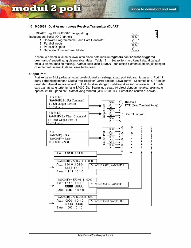
E3165 / UNIT 3 / 99
ASSEMBLY LANGUAGE
12. MC68681 Dual Asynchronous Receiver/Transmitter (DUART)
DUART bagi FLIGHT-68K mengandungi: Independent Serial I/O Channels
1 Software Programmable Baud Rate Generator 6 Parallel Inputs 8 Parallel Outputs 1 Separate Counter/Timer Mode
Kesemua peranti ini akan dikawal atau diberi data melalui registers dan ‘address-triggered commands” seperti yang disenaraikan dalam Table 12.1. Setiap item itu dikenali atau dipanggil melalui alamat masing-masing. Alamat asas ialah $A00001 dan setiap elemen akan dirujuk dengan ofset tertentu merujuk alamat asas berkenaan.
Output Port Port keluaran 8-bit pelbagai-tugas boleh digunakan sebagai suatu port keluaran tugas am. Port ini perlu berganding dengan Output Port Register (OPR) sebagai kawalannya. Kesemua bit OPR boleh diset atau direset secara individu. Suatu bit diset dengan melaksanakan satu operasi WRITE pada satu alamat yang tertentu (iaitu $A0001D). Begitu juga suatu bit direst dengan melaksanakan satu operasi WRITE pada satu alamat yang tertentu (iaitu $A0001F). Perhatikan contoh di bawah:
OP
7
O P 6 O P 5
O P 4 O P 3
O P 2
O P 0
O P 1
Outp
ut
Port
OP7 OP6 OP5 OP4 OP3 OP2
OP0 OP1
OPR (8 bit)
($A0001D) Bit Set Command
1 = Set Output Port Bit
0 = Tak ubah OPR (8 bit)
($A0001F) Bit Clear Command
1 =Reset Output Port Bit
0 = Tak ubah
Reserved
DTR (Data Terminal Relay)
General Purpose
Outp
ut
Port
OP7 OP6 OP5 OP4 OP3 OP2
OP0 OP1 OPR
($A0001D) = Set
($A0001F) = Reset
1111 0000 = $F0
0 1 0 1 0 1 0 1
($A0001D) = $F0 =1111 0000
Asal: 1 01 0 1 01 0 SSSS UUUU
Baru: 1 1 11 10 1 0
0 1 0 1 1 1 1 1
($A0001F) = $F0 =1111 0000
Asal: 1 11 1 1 0 1 0 RRRR UUUU
Baru: 0000 1 0 1 0
0 1 0 1 0 0 0 0
Asal: 1 01 0 1 01 0
($A0001D) = $80 =1000 0000
Asal: 0000 1 0 1 0 SUUU UUUU
Baru: 1 000 10 1 0
0 1 0 1 0 0 0 1
MOVE.B #$F0, $A0001D.L
MOVE.B #$F0, $A0001F.L
MOVE.B #$80, $A0001D.L
http://modul2poli.blogspot.com/
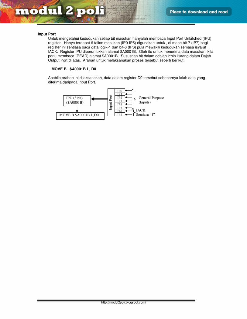
E3165 / UNIT 3 / 100
ASSEMBLY LANGUAGE
Input Port
Untuk mengetahui kedudukan setiap bit masukan hanyalah membaca Input Port Unlatched (IPU) register. Hanya terdapat 6 talian masukan (IP0-IP5) digunakan untuk , di mana bit-7 (IP7) bagi register ini sentiasa baca data logik-1 dan bit-6 (IP6) pula mewakili kedudukan semasa isyarat IACK. Register IPU diperuntukkan alamat $A0001B. Oleh itu untuk menerima data masukan, kita perlu membaca (READ) alamat $A0001B. Sususnan bit dalam adalah lebih kurang dalam Rajah Output Port di atas. Arahan untuk melaksanakan proses tersebut seperti berikut: MOVE.B $A0001B.L, D0 Apabila arahan ini dilaksanakan, data dalam register D0 tersebut sebenarnya ialah data yang diterima daripada Input Port.
Inp
ut
Port
IP7 IP6 IP5 IP4 IP3 IP2
IP0 IP1
IPU (8 bit)
($A0001B) IACK
Sentiasa “1”
General Purpose
(Inputs)
MOVE.B $A0001B.L,D0
http://modul2poli.blogspot.com/
E3165 / UNIT 4 / 1
MOD PENGALAMATAN DAN PENGATURCARAAN
Objektif Am:
Mengetahui dan memahami mod pengalamatan dan pengaturcaraan.
Objektif Khusus:
Pada akhir unit ini, anda seharusnya dapat:
4.1 mengklasifikasikan dan menghuraikan mod pengalamatan 4.2 menerangkan konsep pengaturcaraan 4.3 membincangkan struktur perlaksanaan pengaturcaraan
UNIT 4
OBJEKTIF
http://modul2poli.blogspot.com/
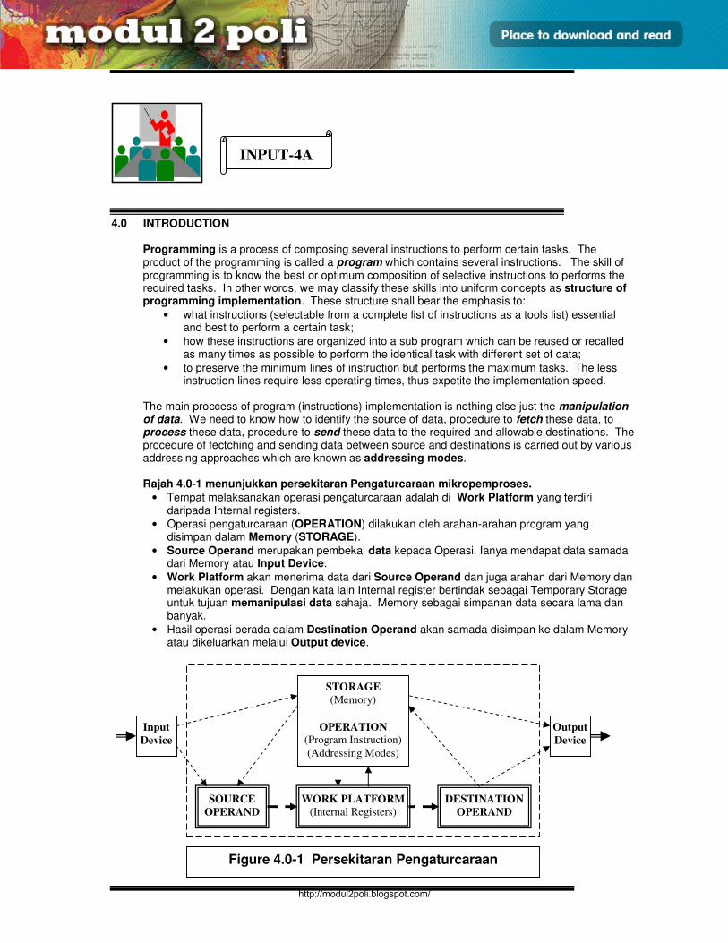
E3165 / UNIT 4 / 2
MOD PENGALAMATAN DAN PENGATURCARAAN
4.0 INTRODUCTION
Programming is a process of composing several instructions to perform certain tasks. The product of the programming is called a program which contains several instructions. The skill of programming is to know the best or optimum composition of selective instructions to performs the required tasks. In other words, we may classify these skills into uniform concepts as structure of programming implementation. These structure shall bear the emphasis to:
• what instructions (selectable from a complete list of instructions as a tools list) essential and best to perform a certain task;
• how these instructions are organized into a sub program which can be reused or recalled as many times as possible to perform the identical task with different set of data;
• to preserve the minimum lines of instruction but performs the maximum tasks. The less instruction lines require less operating times, thus expetite the implementation speed.
The main proccess of program (instructions) implementation is nothing else just the manipulation of data. We need to know how to identify the source of data, procedure to fetch these data, to process these data, procedure to send these data to the required and allowable destinations. The procedure of fectching and sending data between source and destinations is carried out by various addressing approaches which are known as addressing modes. Rajah 4.0-1 menunjukkan persekitaran Pengaturcaraan mikropemproses.
• Tempat melaksanakan operasi pengaturcaraan adalah di Work Platform yang terdiri daripada Internal registers.
• Operasi pengaturcaraan (OPERATION) dilakukan oleh arahan-arahan program yang disimpan dalam Memory (STORAGE).
• Source Operand merupakan pembekal data kepada Operasi. Ianya mendapat data samada dari Memory atau Input Device.
• Work Platform akan menerima data dari Source Operand dan juga arahan dari Memory dan melakukan operasi. Dengan kata lain Internal register bertindak sebagai Temporary Storage untuk tujuan memanipulasi data sahaja. Memory sebagai simpanan data secara lama dan banyak.
• Hasil operasi berada dalam Destination Operand akan samada disimpan ke dalam Memory atau dikeluarkan melalui Output device.
INPUT-4A
OPERATION
(Program Instruction)
(Addressing Modes)
SOURCE
OPERAND
DESTINATION
OPERAND
STORAGE
(Memory)
WORK PLATFORM
(Internal Registers)
Input
Device
Output
Device
Figure 4.0-1 Persekitaran Pengaturcaraan
http://modul2poli.blogspot.com/
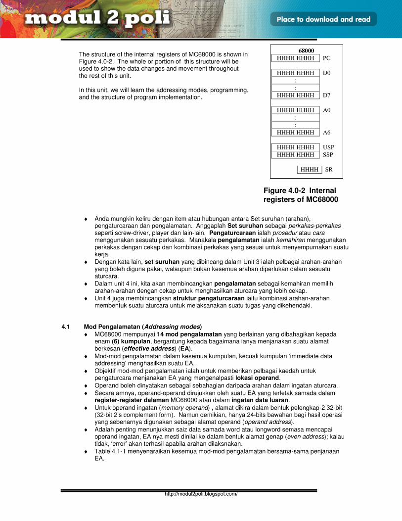
E3165 / UNIT 4 / 3
MOD PENGALAMATAN DAN PENGATURCARAAN
The structure of the internal registers of MC68000 is shown in Figure 4.0-2. The whole or portion of this structure will be used to show the data changes and movement throughout the rest of this unit. In this unit, we will learn the addressing modes, programming, and the structure of program implementation.
♦ Anda mungkin keliru dengan item atau hubungan antara Set suruhan (arahan), pengaturcaraan dan pengalamatan. Anggaplah Set suruhan sebagai perkakas-perkakas seperti screw-driver, player dan lain-lain. Pengaturcaraan ialah prosedur atau cara menggunakan sesuatu perkakas. Manakala pengalamatan ialah kemahiran menggunakan perkakas dengan cekap dan kombinasi perkakas yang sesuai untuk menyempurnakan suatu kerja.
♦ Dengan kata lain, set suruhan yang dibincang dalam Unit 3 ialah pelbagai arahan-arahan yang boleh diguna pakai, walaupun bukan kesemua arahan diperlukan dalam sesuatu aturcara.
♦ Dalam unit 4 ini, kita akan membincangkan pengalamatan sebagai kemahiran memilih arahan-arahan dengan cekap untuk menghasilkan aturcara yang lebih cekap.
♦ Unit 4 juga membincangkan struktur pengaturcaraan iaitu kombinasi arahan-arahan membentuk suatu aturcara untuk melaksanakan suatu tugas yang dikehendaki.
4.1 Mod Pengalamatan (Addressing modes)
♦ MC68000 mempunyai 14 mod pengalamatan yang berlainan yang dibahagikan kepada enam (6) kumpulan, bergantung kepada bagaimana ianya menjanakan suatu alamat berkesan (effective address) (EA).
♦ Mod-mod pengalamatan dalam kesemua kumpulan, kecuali kumpulan ‘immediate data addressing’ menghasilkan suatu EA.
♦ Objektif mod-mod pengalamatan ialah untuk memberikan pelbagai kaedah untuk pengaturcara menjanakan EA yang mengenalpasti lokasi operand.
♦ Operand boleh dinyatakan sebagai sebahagian daripada arahan dalam ingatan aturcara.
♦ Secara amnya, operand-operand dirujukkan oleh suatu EA yang terletak samada dalam register-register dalaman MC68000 atau dalam ingatan data luaran.
♦ Untuk operand ingatan (memory operand) , alamat dikira dalam bentuk pelengkap-2 32-bit (32-bit 2’s complement form). Namun demikian, hanya 24-bits bawahan bagi hasil operasi yang sebenarnya digunakan sebagai alamat operand (operand address).
♦ Adalah penting menunjukkan saiz data samada word atau longword semasa mencapai operand ingatan, EA nya mesti dinilai ke dalam bentuk alamat genap (even address); kalau tidak, ‘error’ akan terhasil apabila arahan dilaksnakan.
♦ Table 4.1-1 menyenaraikan kesemua mod-mod pengalamatan bersama-sama penjanaan EA.
68000
HHHH HHHH PC
HHHH HHHH D0
:
:
HHHH HHHH D7
HHHH HHHH A0
:
:
HHHH HHHH A6
HHHH HHHH USP
HHHH HHHH SSP
HHHH SR
Figure 4.0-2 Internal registers of MC68000
http://modul2poli.blogspot.com/
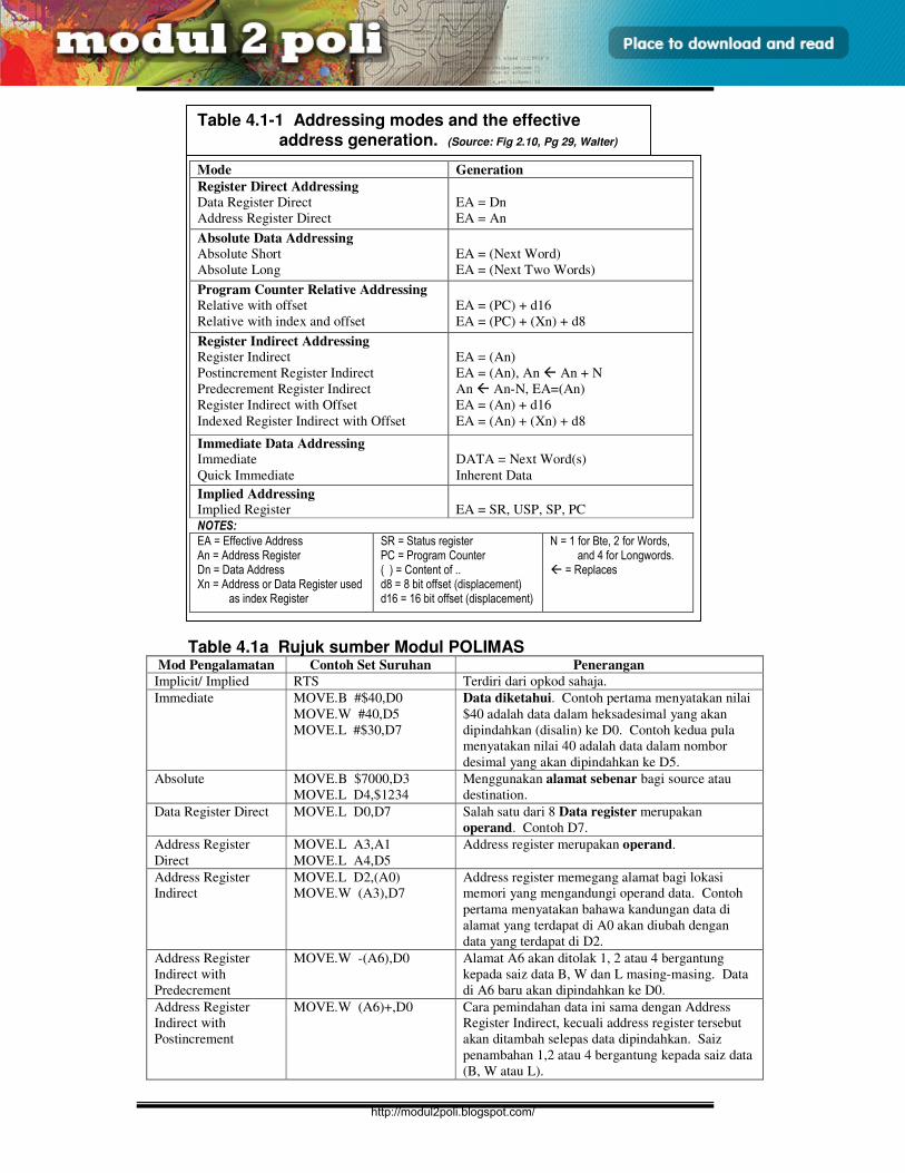
E3165 / UNIT 4 / 4
MOD PENGALAMATAN DAN PENGATURCARAAN
Table 4.1a Rujuk sumber Modul POLIMAS
Table 4.1-1 Addressing modes and the effective address generation. (Source: Fig 2.10, Pg 29, Walter)
Mode Generation
Register Direct Addressing
Data Register Direct
Address Register Direct
EA = Dn
EA = An
Absolute Data Addressing
Absolute Short
Absolute Long
EA = (Next Word)
EA = (Next Two Words)
Program Counter Relative Addressing
Relative with offset
Relative with index and offset
EA = (PC) + d16
EA = (PC) + (Xn) + d8
Register Indirect Addressing
Register Indirect
Postincrement Register Indirect
Predecrement Register Indirect
Register Indirect with Offset
Indexed Register Indirect with Offset
EA = (An)
EA = (An), An An + N
An An-N, EA=(An)
EA = (An) + d16
EA = (An) + (Xn) + d8
Immediate Data Addressing Immediate
Quick Immediate
DATA = Next Word(s)
Inherent Data
Implied Addressing Implied Register
EA = SR, USP, SP, PC
NOTES:
EA = Effective Address An = Address Register Dn = Data Address Xn = Address or Data Register used
as index Register
SR = Status register PC = Program Counter ( ) = Content of .. d8 = 8 bit offset (displacement) d16 = 16 bit offset (displacement)
N = 1 for Bte, 2 for Words, and 4 for Longwords.
= Replaces
Mod Pengalamatan Contoh Set Suruhan Penerangan
Implicit/ Implied RTS Terdiri dari opkod sahaja.
Immediate MOVE.B #$40,D0
MOVE.W #40,D5
MOVE.L #$30,D7
Data diketahui. Contoh pertama menyatakan nilai
$40 adalah data dalam heksadesimal yang akan
dipindahkan (disalin) ke D0. Contoh kedua pula
menyatakan nilai 40 adalah data dalam nombor
desimal yang akan dipindahkan ke D5.
Absolute MOVE.B $7000,D3
MOVE.L D4,$1234
Menggunakan alamat sebenar bagi source atau
destination.
Data Register Direct MOVE.L D0,D7
Salah satu dari 8 Data register merupakan
operand. Contoh D7.
Address Register
Direct
MOVE.L A3,A1
MOVE.L A4,D5
Address register merupakan operand.
Address Register
Indirect
MOVE.L D2,(A0)
MOVE.W (A3),D7
Address register memegang alamat bagi lokasi
memori yang mengandungi operand data. Contoh
pertama menyatakan bahawa kandungan data di
alamat yang terdapat di A0 akan diubah dengan
data yang terdapat di D2.
Address Register
Indirect with
Predecrement
MOVE.W -(A6),D0 Alamat A6 akan ditolak 1, 2 atau 4 bergantung
kepada saiz data B, W dan L masing-masing. Data
di A6 baru akan dipindahkan ke D0.
Address Register
Indirect with
Postincrement
MOVE.W (A6)+,D0 Cara pemindahan data ini sama dengan Address
Register Indirect, kecuali address register tersebut
akan ditambah selepas data dipindahkan. Saiz
penambahan 1,2 atau 4 bergantung kepada saiz data
(B, W atau L).
http://modul2poli.blogspot.com/
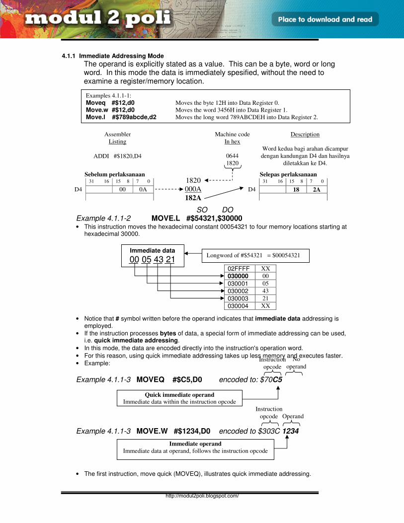
E3165 / UNIT 4 / 5
MOD PENGALAMATAN DAN PENGATURCARAAN
4.1.1 Immediate Addressing Mode
The operand is explicitly stated as a value. This can be a byte, word or long word. In this mode the data is immediately spesified, without the need to examine a register/memory location.
SO DO Example 4.1.1-2 MOVE.L #$54321,$30000 • This instruction moves the hexadecimal constant 00054321 to four memory locations starting at
hexadecimal 30000.
• Notice that # symbol written before the operand indicates that immediate data addressing is employed.
• If the instruction processes bytes of data, a special form of immediate addressing can be used, i.e. quick immediate addressing.
• In this mode, the data are encoded directly into the instruction's operation word.
• For this reason, using quick immediate addressing takes up less memory and executes faster.
• Example:
Example 4.1.1-3 MOVEQ #$C5,D0 encoded to: $70C5
Example 4.1.1-3 MOVE.W #$1234,D0 encoded to $303C 1234
• The first instruction, move quick (MOVEQ), illustrates quick immediate addressing.
Assembler
Listing
ADDI #$1820,D4
Description
Word kedua bagi arahan dicampur
dengan kandungan D4 dan hasilnya
diletakkan ke D4.
31 16 15 8 7 0
D4 00 0A
1820
000A
182A
Machine code
In hex
0644
1820
31 16 15 8 7 0
D4 18 2A
Sebelum perlaksanaan Selepas perlaksanaan
02FFFF XX
030000 00
030001 05
030002 43
030003 21
030004 XX
Immediate data
00 05 43 21 Longword of #$54321 = $00054321
Quick immediate operand Immediate data within the instruction opcode
Immediate operand
Immediate data at operand, follows the instruction opcode
Instruction
opcode
No
operand
Instruction
opcode Operand
Examples 4.1.1-1:
Moveq #$12,d0 Moves the byte 12H into Data Register 0.
Move.w #$12,d0 Moves the word 3456H into Data Register 1.
Move.l #$789abcde,d2 Moves the long word 789ABCDEH into Data Register 2.
http://modul2poli.blogspot.com/
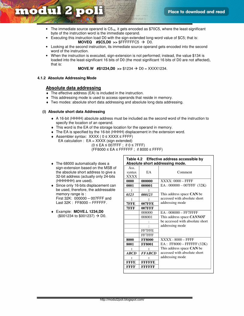
E3165 / UNIT 4 / 6
MOD PENGALAMATAN DAN PENGATURCARAAN
• The immediate source operand is C516, it gets encoded as $70C5, where the least-significant byte of the instruction word is the immediate operand.
• Executing this instruction load D0 with the sign-extended long-word value of $C5; that is: MOVEQ #$C5,D0 >> $FFFFFFC5 D0.
• Looking at the second instruction, its immediate source operand gets encoded into the second word of the instruction.
• When the instruction is executed, sign-extension is not performed; instead, the value $134 is loaded into the least-significant 16 bits of D0 (the most significant 16 bits of D0 are not affected), that is:
MOVE.W #$1234,D0 >> $1234 D0 = XXXX1234.
4.1.2 Absolute Addressing Mode
Absolute data addressing ♦ The effective address (EA) is included in the instruction.
♦ This addressing mode is used to access operands that reside in memory.
♦ Two modes: absolute short data addressing and absolute long data addressing.
(i) Absolute short data Addressing
♦ A 16-bit (HHHH) absolute address must be included as the second word of the instruction to specify the location of an operand.
♦ This word is the EA of the storage location for the operand in memory.
♦ The EA is specified by the 16-bit (HHHH) displacement in the extension word.
♦ Assembler syntax: XXXX ( 0 ≤ XXXX ≤ FFFF) EA calculation : EA = XXXX (sign extended) (0 ≤ EA ≤ 007FFF ; if 0 ≤ 7FFF) (FF8000 ≤ EA ≤ FFFFFF ; if 8000 ≤ FFFF)
♦ The 68000 automatically does a
sign-extension based on the MSB of the absolute short address to give a 32-bit address (actually only 24-bits (HHHHHH) are used).
♦ Since only 16-bits displacement can be used, therefore, the addressable memory range is :
First 32K: 000000 – 007FFF and Last 32K : FF8000 – FFFFFF.
♦ Example: MOVE.L 1234,D0 ($001234 to $001237) D0.
Table 4.2 Effective address accessible by Absolute short addressing mode.
Ass.
syntax
XXXX
EA
Comment
0000 000000 XXXX: 0000 – FFFF
EA : 000000 – 007FFF (32K)
This address space CAN be
accessed with absolute short
addressing mode
0001 000001
: :
0123 000123
: :
7FFE 007FFE
7FFF 007FFF
008000 EA : 008000 – FF7FFFF
This address space CANNOT
be accessed with absolute short
addressing mode
008001
:
:
FF7FFE
FF7FFF
8000 FF8000 XXXX : 8000 – FFFF
EA : FF8000 – FFFFFF (32K)
This address space CAN be
accessed with absolute short
addressing mode
8001 FF8001
: :
ABCD FFABCD
: :
FFFE FFFFFE
FFFF FFFFFF
http://modul2poli.blogspot.com/
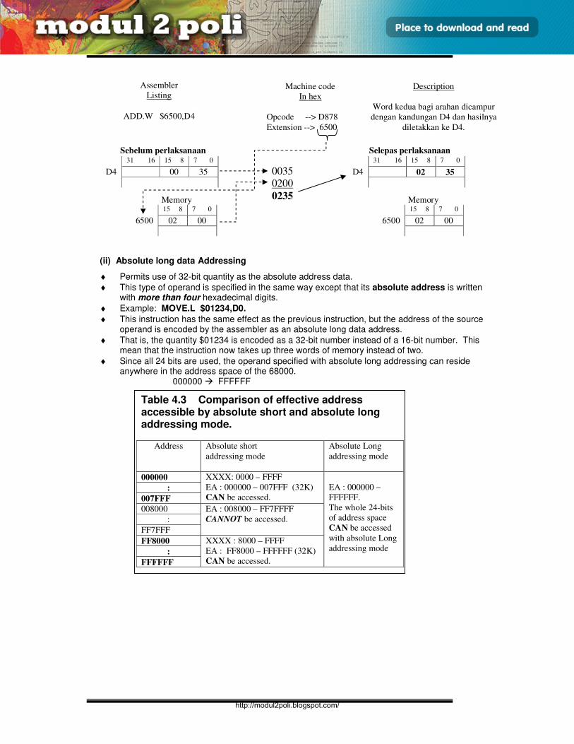
E3165 / UNIT 4 / 7
MOD PENGALAMATAN DAN PENGATURCARAAN
(ii) Absolute long data Addressing
♦ Permits use of 32-bit quantity as the absolute address data.
♦ This type of operand is specified in the same way except that its absolute address is written with more than four hexadecimal digits.
♦ Example: MOVE.L $01234,D0.
♦ This instruction has the same effect as the previous instruction, but the address of the source operand is encoded by the assembler as an absolute long data address.
♦ That is, the quantity $01234 is encoded as a 32-bit number instead of a 16-bit number. This mean that the instruction now takes up three words of memory instead of two.
♦ Since all 24 bits are used, the operand specified with absolute long addressing can reside anywhere in the address space of the 68000.
000000 FFFFFF
Assembler
Listing
ADD.W $6500,D4
Description
Word kedua bagi arahan dicampur
dengan kandungan D4 dan hasilnya
diletakkan ke D4.
31 16 15 8 7 0
D4 00 35
0035
0200
0235
Machine code
In hex
Opcode --> D878
Extension --> 6500
31 16 15 8 7 0
D4 02 35
Sebelum perlaksanaan Selepas perlaksanaan
Memory 15 8 7 0
6500 02 00
Memory 15 8 7 0
6500 02 00
Table 4.3 Comparison of effective address accessible by absolute short and absolute long addressing mode.
Address Absolute short
addressing mode
Absolute Long
addressing mode
000000 XXXX: 0000 – FFFF
EA : 000000 – 007FFF (32K)
CAN be accessed.
EA : 000000 –
FFFFFF.
The whole 24-bits
of address space
CAN be accessed
with absolute Long
addressing mode
:
007FFF
008000 EA : 008000 – FF7FFFF
CANNOT be accessed. :
FF7FFF
FF8000 XXXX : 8000 – FFFF
EA : FF8000 – FFFFFF (32K)
CAN be accessed. :
FFFFFF
http://modul2poli.blogspot.com/
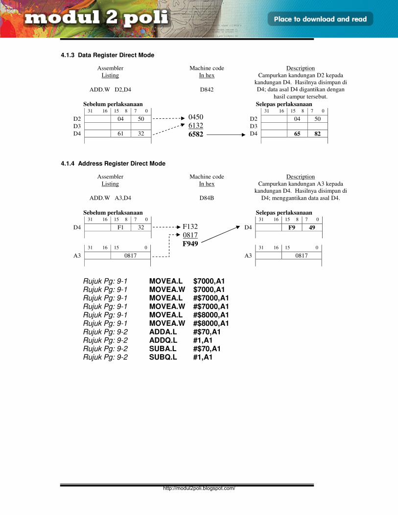
E3165 / UNIT 4 / 8
MOD PENGALAMATAN DAN PENGATURCARAAN
4.1.3 Data Register Direct Mode
4.1.4 Address Register Direct Mode
Rujuk Pg: 9-1 MOVEA.L $7000,A1 Rujuk Pg: 9-1 MOVEA.W $7000,A1 Rujuk Pg: 9-1 MOVEA.L #$7000,A1 Rujuk Pg: 9-1 MOVEA.W #$7000,A1 Rujuk Pg: 9-1 MOVEA.L #$8000,A1 Rujuk Pg: 9-1 MOVEA.W #$8000,A1 Rujuk Pg: 9-2 ADDA.L #$70,A1 Rujuk Pg: 9-2 ADDQ.L #1,A1 Rujuk Pg: 9-2 SUBA.L #$70,A1 Rujuk Pg: 9-2 SUBQ.L #1,A1
Assembler
Listing
ADD.W D2,D4
Description
Campurkan kandungan D2 kepada
kandungan D4. Hasilnya disimpan di
D4; data asal D4 digantikan dengan
hasil campur tersebut.
31 16 15 8 7 0
D2 04 50
D3
D4 61 32
0450
6132
6582
Machine code
In hex
D842
Sebelum perlaksanaan Selepas perlaksanaan
31 16 15 8 7 0
D2 04 50
D3
D4 65 82
Assembler
Listing
ADD.W A3,D4
Description
Campurkan kandungan A3 kepada
kandungan D4. Hasilnya disimpan di
D4; menggantikan data asal D4.
Machine code
In hex
D84B
31 16 15 8 7 0
D4 F1 32
F132
0817
F949
31 16 15 8 7 0
D4 F9 49
Sebelum perlaksanaan Selepas perlaksanaan
31 16 15 0
A3 0817
31 16 15 0
A3 0817
http://modul2poli.blogspot.com/
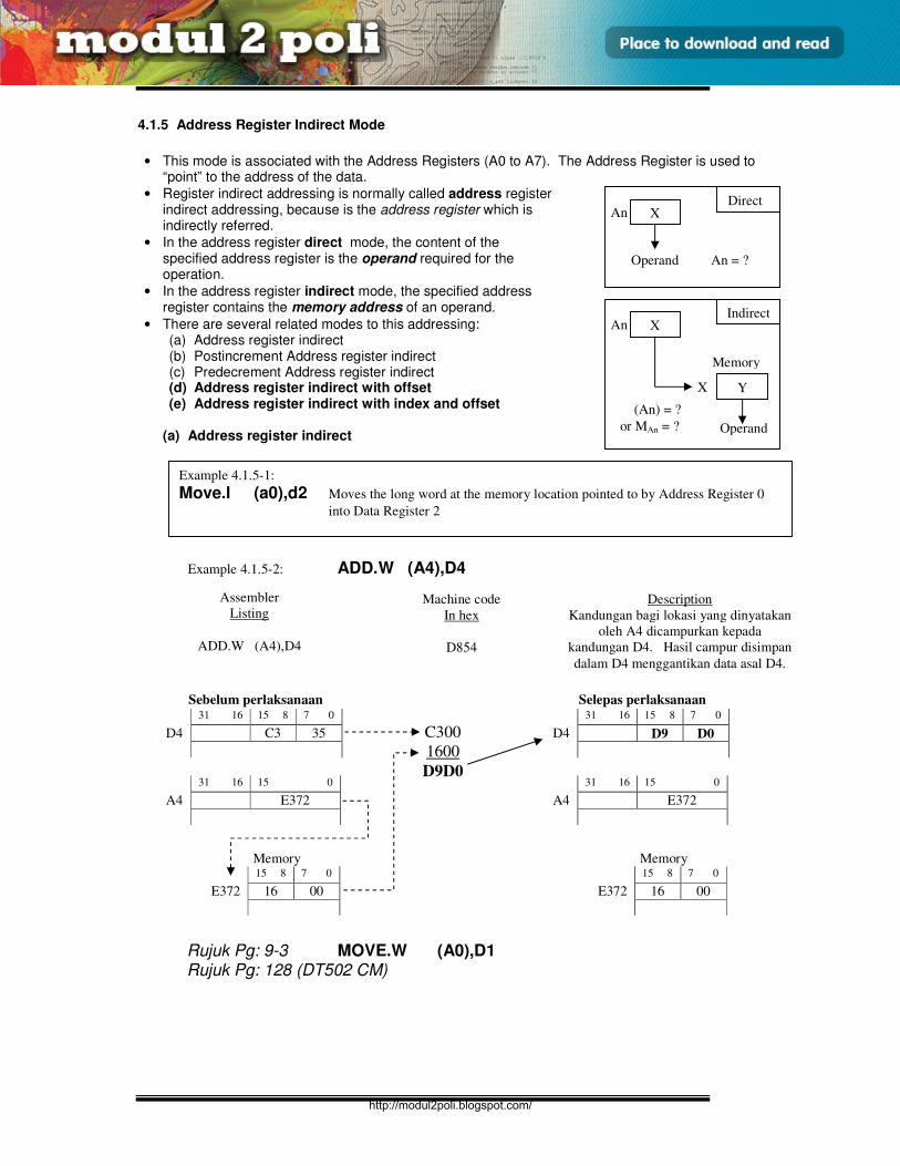
E3165 / UNIT 4 / 9
MOD PENGALAMATAN DAN PENGATURCARAAN
4.1.5 Address Register Indirect Mode
• This mode is associated with the Address Registers (A0 to A7). The Address Register is used to
“point” to the address of the data.
• Register indirect addressing is normally called address register indirect addressing, because is the address register which is indirectly referred.
• In the address register direct mode, the content of the specified address register is the operand required for the operation.
• In the address register indirect mode, the specified address register contains the memory address of an operand.
• There are several related modes to this addressing: (a) Address register indirect (b) Postincrement Address register indirect (c) Predecrement Address register indirect (d) Address register indirect with offset (e) Address register indirect with index and offset
(a) Address register indirect
Example 4.1.5-2: ADD.W (A4),D4
Rujuk Pg: 9-3 MOVE.W (A0),D1 Rujuk Pg: 128 (DT502 CM)
Assembler
Listing
ADD.W (A4),D4
Description
Kandungan bagi lokasi yang dinyatakan
oleh A4 dicampurkan kepada
kandungan D4. Hasil campur disimpan
dalam D4 menggantikan data asal D4.
31 16 15 8 7 0
D4 C3 35
C300
1600
D9D0
Machine code
In hex
D854
31 16 15 8 7 0
D4 D9 D0
Sebelum perlaksanaan Selepas perlaksanaan
Memory 15 8 7 0
E372 16 00
31 16 15 0
A4 E372
Memory 15 8 7 0
E372 16 00
31 16 15 0
A4 E372
X An
Operand
X An
Memory
Y X
Operand
An = ?
(An) = ?
or MAn = ?
Direct
Indirect
Example 4.1.5-1:
Move.l (a0),d2 Moves the long word at the memory location pointed to by Address Register 0
into Data Register 2
http://modul2poli.blogspot.com/
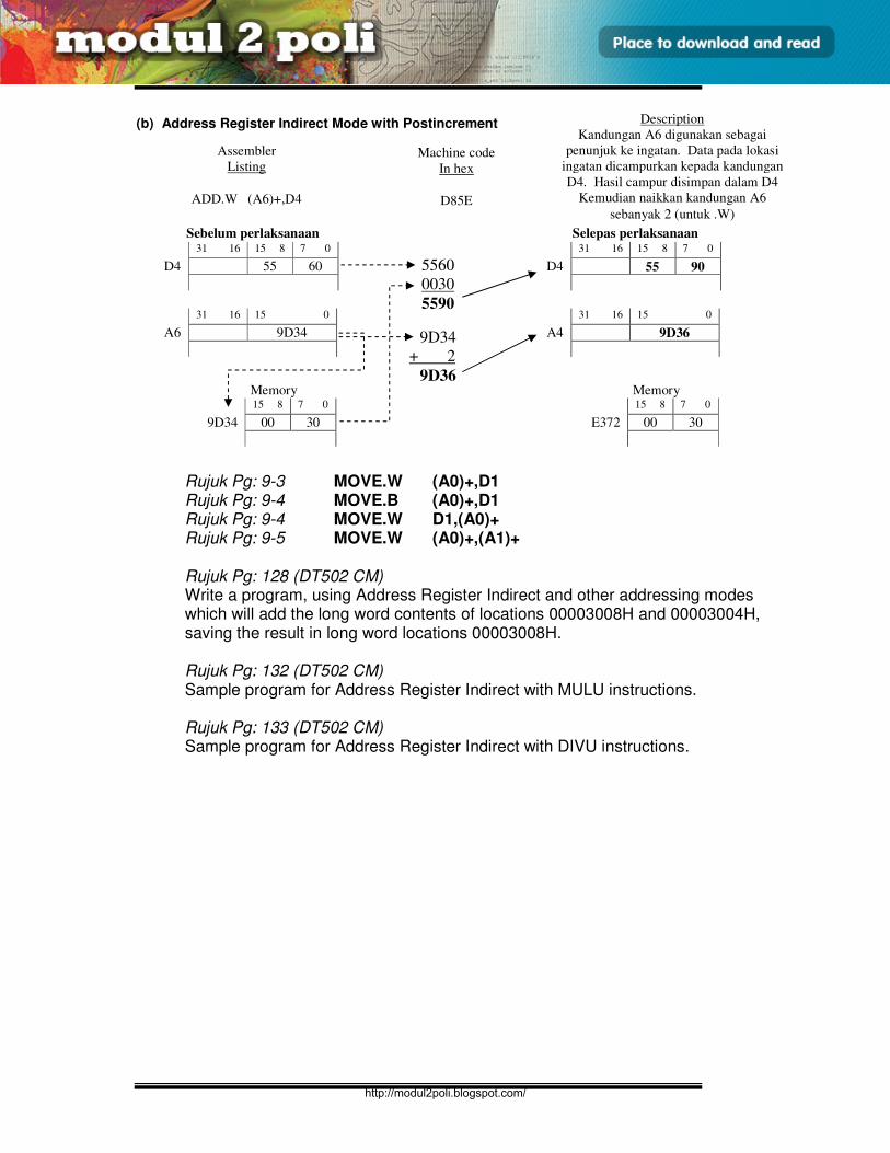
E3165 / UNIT 4 / 10
MOD PENGALAMATAN DAN PENGATURCARAAN
(b) Address Register Indirect Mode with Postincrement
Rujuk Pg: 9-3 MOVE.W (A0)+,D1 Rujuk Pg: 9-4 MOVE.B (A0)+,D1 Rujuk Pg: 9-4 MOVE.W D1,(A0)+ Rujuk Pg: 9-5 MOVE.W (A0)+,(A1)+ Rujuk Pg: 128 (DT502 CM) Write a program, using Address Register Indirect and other addressing modes which will add the long word contents of locations 00003008H and 00003004H, saving the result in long word locations 00003008H. Rujuk Pg: 132 (DT502 CM) Sample program for Address Register Indirect with MULU instructions. Rujuk Pg: 133 (DT502 CM) Sample program for Address Register Indirect with DIVU instructions.
Assembler
Listing
ADD.W (A6)+,D4
Description
Kandungan A6 digunakan sebagai
penunjuk ke ingatan. Data pada lokasi
ingatan dicampurkan kepada kandungan
D4. Hasil campur disimpan dalam D4
Kemudian naikkan kandungan A6
sebanyak 2 (untuk .W)
31 16 15 8 7 0
D4 55 60
5560
0030
5590
Machine code
In hex
D85E
31 16 15 8 7 0
D4 55 90
Sebelum perlaksanaan Selepas perlaksanaan
Memory 15 8 7 0
9D34 00 30
31 16 15 0
A6 9D34
Memory 15 8 7 0
E372 00 30
31 16 15 0
A4 9D36
9D34
+ 2
9D36
http://modul2poli.blogspot.com/
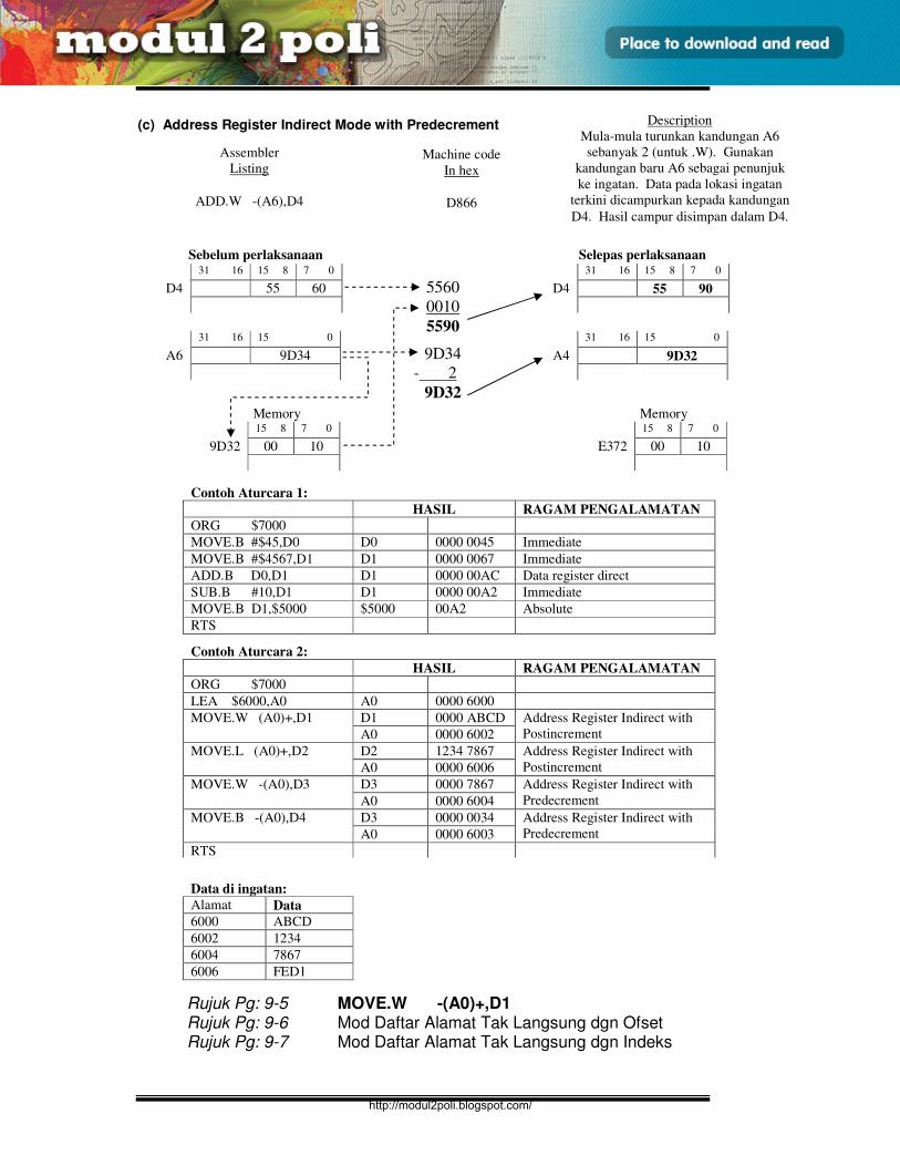
E3165 / UNIT 4 / 11
MOD PENGALAMATAN DAN PENGATURCARAAN
(c) Address Register Indirect Mode with Predecrement
Rujuk Pg: 9-5 MOVE.W -(A0)+,D1 Rujuk Pg: 9-6 Mod Daftar Alamat Tak Langsung dgn Ofset Rujuk Pg: 9-7 Mod Daftar Alamat Tak Langsung dgn Indeks
Assembler
Listing
ADD.W -(A6),D4
Description
Mula-mula turunkan kandungan A6
sebanyak 2 (untuk .W). Gunakan
kandungan baru A6 sebagai penunjuk
ke ingatan. Data pada lokasi ingatan
terkini dicampurkan kepada kandungan
D4. Hasil campur disimpan dalam D4.
31 16 15 8 7 0
D4 55 60
5560
0010
5590
Machine code
In hex
D866
31 16 15 8 7 0
D4 55 90
Sebelum perlaksanaan Selepas perlaksanaan
Memory 15 8 7 0
9D32 00 10
31 16 15 0
A6 9D34
Memory 15 8 7 0
E372 00 10
31 16 15 0
A4 9D32
9D34
- 2
9D32
Contoh Aturcara 1:
HASIL RAGAM PENGALAMATAN
ORG $7000
MOVE.B #$45,D0 D0 0000 0045 Immediate
MOVE.B #$4567,D1 D1 0000 0067 Immediate
ADD.B D0,D1 D1 0000 00AC Data register direct
SUB.B #10,D1 D1 0000 00A2 Immediate
MOVE.B D1,$5000 $5000 00A2 Absolute
RTS
A0 Contoh Aturcara 2:
HASIL RAGAM PENGALAMATAN
ORG $7000
LEA $6000,A0 A0 0000 6000
MOVE.W (A0)+,D1 D1 0000 ABCD Address Register Indirect with
Postincrement A0 0000 6002
MOVE.L (A0)+,D2 D2 1234 7867 Address Register Indirect with
Postincrement A0 0000 6006
MOVE.W -(A0),D3 D3 0000 7867 Address Register Indirect with
Predecrement A0 0000 6004
MOVE.B -(A0),D4 D3 0000 0034 Address Register Indirect with
Predecrement A0 0000 6003
RTS
Data di ingatan:
Alamat Data
6000 ABCD
6002 1234
6004 7867
6006 FED1
http://modul2poli.blogspot.com/
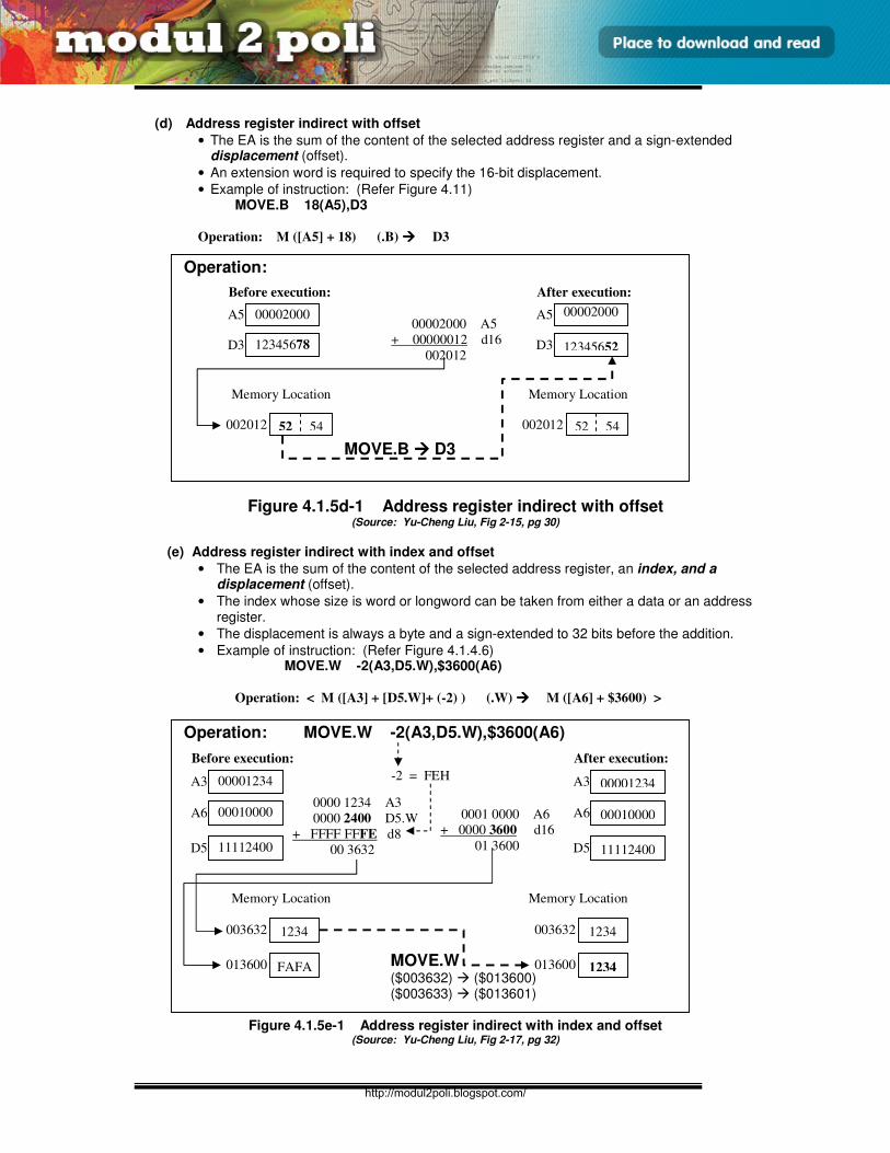
E3165 / UNIT 4 / 12
MOD PENGALAMATAN DAN PENGATURCARAAN
(d) Address register indirect with offset
• The EA is the sum of the content of the selected address register and a sign-extended displacement (offset).
• An extension word is required to specify the 16-bit displacement.
• Example of instruction: (Refer Figure 4.11) MOVE.B 18(A5),D3
Operation: M ([A5] + 18) (.B) D3
Figure 4.1.5d-1 Address register indirect with offset (Source: Yu-Cheng Liu, Fig 2-15, pg 30)
(e) Address register indirect with index and offset
• The EA is the sum of the content of the selected address register, an index, and a displacement (offset).
• The index whose size is word or longword can be taken from either a data or an address register.
• The displacement is always a byte and a sign-extended to 32 bits before the addition.
• Example of instruction: (Refer Figure 4.1.4.6) MOVE.W -2(A3,D5.W),$3600(A6)
Operation: < M ([A3] + [D5.W]+ (-2) ) (.W) M ([A6] + $3600) >
Figure 4.1.5e-1 Address register indirect with index and offset (Source: Yu-Cheng Liu, Fig 2-17, pg 32)
00002000 A5
Before execution:
00002000
A5
After execution:
Memory Location Memory Location
MOVE.B D3
Operation:
002012 52 54 002012 52 54
12345678 D3 12345652 D3
00002000 A5
+ 00000012 d16
002012
00001234 A3
Before execution:
00001234 A3
After execution:
Memory Location Memory Location
MOVE.W ($003632) ($013600) ($003633) ($013601)
Operation: MOVE.W -2(A3,D5.W),$3600(A6)
003632
00010000 A6 00010000 A6 0000 1234 A3
0000 2400 D5.W
+ FFFF FFFE d8
00 3632 11112400 D5 11112400 D5
0001 0000 A6
+ 0000 3600 d16
01 3600
013600
1234
FAFA
003632
013600
1234
1234
-2 = FEH
http://modul2poli.blogspot.com/
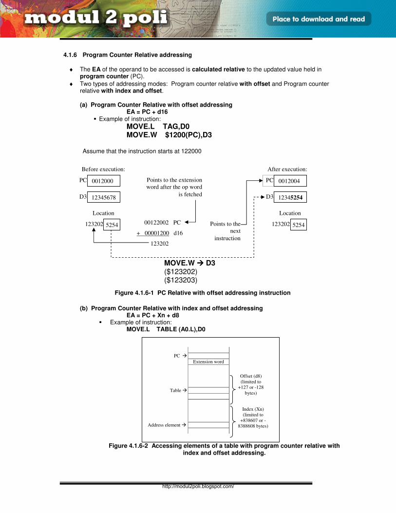
E3165 / UNIT 4 / 13
MOD PENGALAMATAN DAN PENGATURCARAAN
4.1.6 Program Counter Relative addressing
♦ The EA of the operand to be accessed is calculated relative to the updated value held in program counter (PC).
♦ Two types of addressing modes: Program counter relative with offset and Program counter relative with index and offset.
(a) Program Counter Relative with offset addressing EA = PC + d16
Example of instruction:
MOVE.L TAG,D0 MOVE.W $1200(PC),D3
Assume that the instruction starts at 122000
Figure 4.1.6-1 PC Relative with offset addressing instruction
(b) Program Counter Relative with index and offset addressing EA = PC + Xn + d8
Example of instruction: MOVE.L TABLE (A0.L),D0
Figure 4.1.6-2 Accessing elements of a table with program counter relative with index and offset addressing.
0012000 PC
Before execution:
12345678 D3
0012004 PC
After execution:
12345254 D3
00122002 PC
+ 00001200 d16
123202
5254 123202
Points to the extension
word after the op word
is fetched
5254 123202 Points to the
next
instruction
Location Location
MOVE.W D3 ($123202) ($123203)
PC
Extension word
Table
Address element
Offset (d8)
(limited to +127 or -128
bytes)
Index (Xn)
(limited to
+838607 or -
8388608 bytes)
http://modul2poli.blogspot.com/
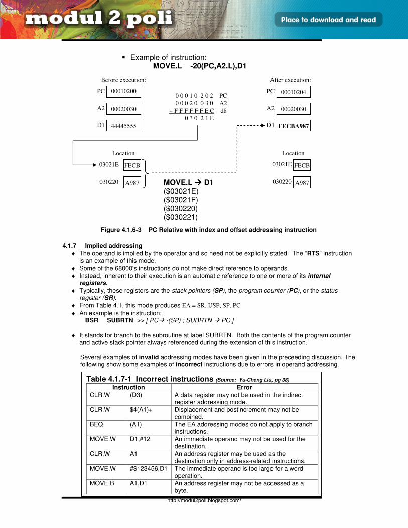
E3165 / UNIT 4 / 14
MOD PENGALAMATAN DAN PENGATURCARAAN
Example of instruction: MOVE.L -20(PC,A2.L),D1
Figure 4.1.6-3 PC Relative with index and offset addressing instruction
4.1.7 Implied addressing
♦ The operand is implied by the operator and so need not be explicitly stated. The “RTS” instruction is an example of this mode.
♦ Some of the 68000's instructions do not make direct reference to operands.
♦ Instead, inherent to their execution is an automatic reference to one or more of its internal registers.
♦ Typically, these registers are the stack pointers (SP), the program counter (PC), or the status register (SR).
♦ From Table 4.1, this mode produces EA = SR, USP, SP, PC
♦ An example is the instruction: BSR SUBRTN >> [ PC -(SP) ; SUBRTN PC ]
♦ It stands for branch to the subroutine at label SUBRTN. Both the contents of the program counter and active stack pointer always referenced during the extension of this instruction.
Several examples of invalid addressing modes have been given in the preceeding discussion. The following show some examples of incorrect instructions due to errors in operand addressing.
00010200 PC
Before execution:
44445555 D1
00010204 PC
After execution:
FECBA987 D1
0 0 0 1 0 2 0 2 PC
0 0 0 2 0 0 3 0 A2
+ F F F F F F E C d8
0 3 0 2 1 E
FECB 03021E FECB 03021E
Location Location
MOVE.L D1 ($03021E) ($03021F) ($030220) ($030221)
00020030 A2 00020030 A2
A987 030220 A987 030220
Table 4.1.7-1 Incorrect instructions (Source: Yu-Cheng Liu, pg 38) Instruction Error
CLR.W (D3) A data register may not be used in the indirect register addressing mode.
CLR.W $4(A1)+ Displacement and postincrement may not be combined.
BEQ (A1) The EA addressing modes do not apply to branch instructions.
MOVE.W D1,#12 An immediate operand may not be used for the destination.
CLR.W A1 An address register may be used as the destination only in address-related instructions.
MOVE.W #$123456,D1 The immediate operand is too large for a word operation.
MOVE.B A1,D1 An address register may not be accessed as a byte.
http://modul2poli.blogspot.com/
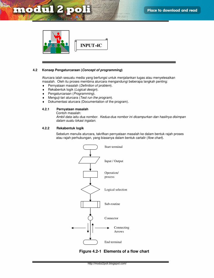
E3165 / UNIT 4 / 15
MOD PENGALAMATAN DAN PENGATURCARAAN
4.2 Konsep Pengaturcaraan (Concept of programming)
Aturcara ialah sesuatu media yang berfungsi untuk menjalankan tugas atau menyelesaikan masalah. Oleh itu proses membina aturcara mengandungi beberapa langkah penting:
♦ Pernyataan masalah (Definition of problem).
♦ Rekabentuk logik (Logical design).
♦ Pengaturcaraan (Programming).
♦ Menguji-lari aturcara (Test run the program).
♦ Dokumentasi aturcara (Documentation of the program). 4.2.1 Pernyataan masalah
Contoh masalah: Ambil data iaitu dua nombor. Kedua-dua nombor ini dicampurkan dan hasilnya disimpan dalam suatu lokasi ingatan.
4.2.2 Rekabentuk logik
Sebelum menulis aturcara, takrifkan pernyataan masalah ke dalam bentuk rajah proses atau rajah perhubungan, yang biasanya dalam bentuk cartalir (flow chart).
Figure 4.2-1 Elements of a flow chart
INPUT-4C
Start terminal
Input / Output
Operation/
process
Logical selection
Sub-routine
Connector
Connecting
Arrows
End terminal
http://modul2poli.blogspot.com/
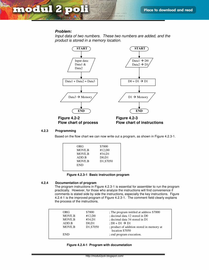
E3165 / UNIT 4 / 16
MOD PENGALAMATAN DAN PENGATURCARAAN
Problem: Input data of two numbers. These two numbers are added, and the product is stored in a memory location.
4.2.3 Programming
Based on the flow chart we can now write out a program, as shown in Figure 4.2.3-1.
Figure 4.2.3-1 Basic instruction program
4.2.4 Documentation of program
The program instructions in Figure 4.2.3-1 is essential for assembler to run the program practically. However, for those who analyze the instructions will find convenience if comments is stated side by side the instructions, especially the key instructions. Figure 4.2.4-1 is the improved program of Figure 4.2.3-1. The comment field clearly explains the process of the instructions.
Figure 4.2.4-1 Program with documetation
Figure 4.2-2 Flow chart of process
START
Input data:
Data1 &
Data2
Data1 + Data2 = Data3
Data3 Memory
END
START
Data1 D0
Data2 D1
D0 + D1 D1
D1 Memory
END
Figure 4.2-3 Flow chart of instructions
ORG $7000
MOVE.B #12,D0
MOVE.B #34,D1
ADD.B D0,D1
MOVE.B D1,$7050
END
ORG $7000 ; The program initiled at address $7000
MOVE.B #12,D0 ; decimal data 12 stored in D0
MOVE.B #34,D1 ; decimal data 34 stored in D1
ADD.B D0,D1 ; D0 + D1 D1
MOVE.B D1,$7050 ; product of addition stored in memory at
location $7050
END ; end program execution.
http://modul2poli.blogspot.com/
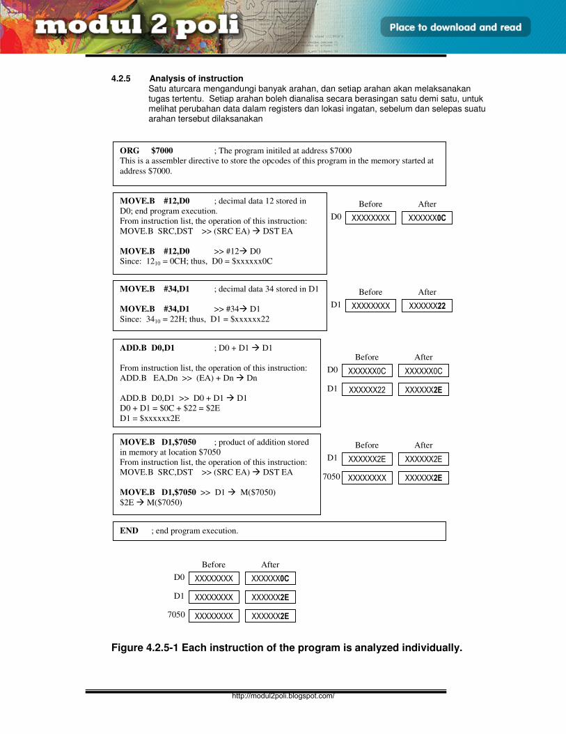
E3165 / UNIT 4 / 17
MOD PENGALAMATAN DAN PENGATURCARAAN
4.2.5 Analysis of instruction
Satu aturcara mengandungi banyak arahan, dan setiap arahan akan melaksanakan tugas tertentu. Setiap arahan boleh dianalisa secara berasingan satu demi satu, untuk melihat perubahan data dalam registers dan lokasi ingatan, sebelum dan selepas suatu arahan tersebut dilaksanakan
Figure 4.2.5-1 Each instruction of the program is analyzed individually.
ADD.B D0,D1 ; D0 + D1 D1
From instruction list, the operation of this instruction:
ADD.B EA,Dn >> (EA) + Dn Dn
ADD.B D0,D1 >> D0 + D1 D1
D0 + D1 = $0C + $22 = $2E
D1 = $xxxxxx2E
ORG $7000 ; The program initiled at address $7000
This is a assembler directive to store the opcodes of this program in the memory started at
address $7000.
MOVE.B #12,D0 ; decimal data 12 stored in
D0; end program execution.
From instruction list, the operation of this instruction:
MOVE.B SRC,DST >> (SRC EA) DST EA
MOVE.B #12,D0 >> #12 D0
Since: 1210 = 0CH; thus, D0 = $xxxxxx0C
MOVE.B #34,D1 ; decimal data 34 stored in D1
MOVE.B #34,D1 >> #34 D1
Since: 3410 = 22H; thus, D1 = $xxxxxx22
D0 XXXXXXXX XXXXXX0C
Before After
D1 XXXXXXXX XXXXXX22
Before After
D0 XXXXXX0C XXXXXX0C
Before After
D1 XXXXXX22 XXXXXX2E
MOVE.B D1,$7050 ; product of addition stored
in memory at location $7050
From instruction list, the operation of this instruction:
MOVE.B SRC,DST >> (SRC EA) DST EA
MOVE.B D1,$7050 >> D1 M($7050)
$2E M($7050)
D1 XXXXXX2E XXXXXX2E
Before After
7050 XXXXXXXX XXXXXX2E
END ; end program execution.
D1 XXXXXXXX XXXXXX2E
Before After
7050 XXXXXXXX XXXXXX2E
D0 XXXXXXXX XXXXXX0C
http://modul2poli.blogspot.com/
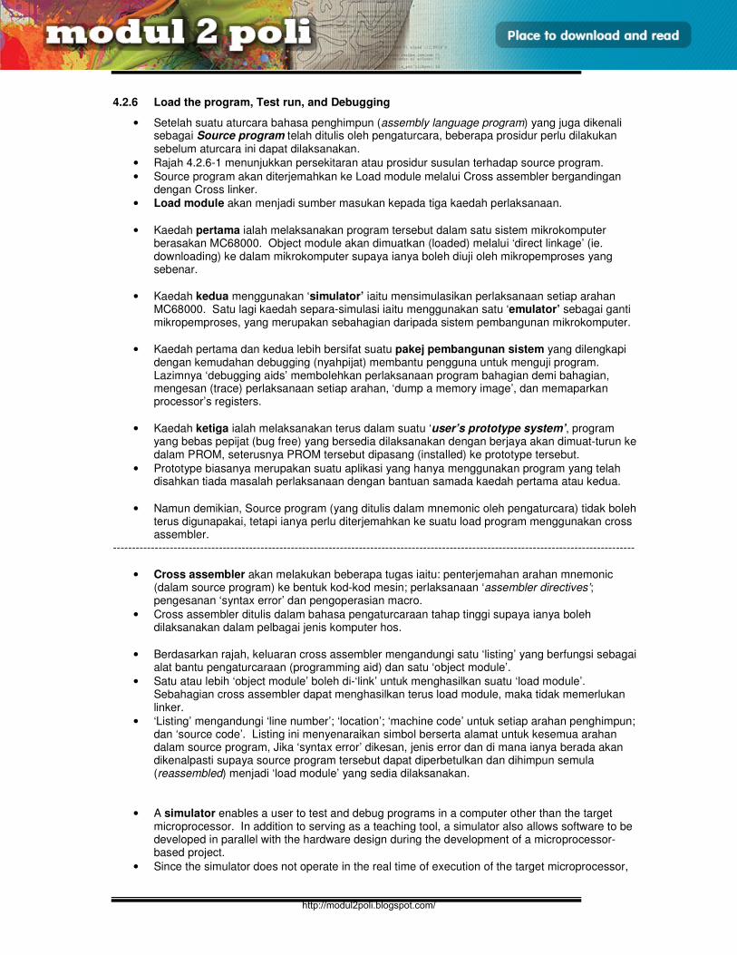
E3165 / UNIT 4 / 18
MOD PENGALAMATAN DAN PENGATURCARAAN
4.2.6 Load the program, Test run, and Debugging
• Setelah suatu aturcara bahasa penghimpun (assembly language program) yang juga dikenali sebagai Source program telah ditulis oleh pengaturcara, beberapa prosidur perlu dilakukan sebelum aturcara ini dapat dilaksanakan.
• Rajah 4.2.6-1 menunjukkan persekitaran atau prosidur susulan terhadap source program.
• Source program akan diterjemahkan ke Load module melalui Cross assembler bergandingan dengan Cross linker.
• Load module akan menjadi sumber masukan kepada tiga kaedah perlaksanaan.
• Kaedah pertama ialah melaksanakan program tersebut dalam satu sistem mikrokomputer berasakan MC68000. Object module akan dimuatkan (loaded) melalui ‘direct linkage’ (ie. downloading) ke dalam mikrokomputer supaya ianya boleh diuji oleh mikropemproses yang sebenar.
• Kaedah kedua menggunakan ‘simulator’ iaitu mensimulasikan perlaksanaan setiap arahan MC68000. Satu lagi kaedah separa-simulasi iaitu menggunakan satu ‘emulator’ sebagai ganti mikropemproses, yang merupakan sebahagian daripada sistem pembangunan mikrokomputer.
• Kaedah pertama dan kedua lebih bersifat suatu pakej pembangunan sistem yang dilengkapi dengan kemudahan debugging (nyahpijat) membantu pengguna untuk menguji program. Lazimnya ‘debugging aids’ membolehkan perlaksanaan program bahagian demi bahagian, mengesan (trace) perlaksanaan setiap arahan, ‘dump a memory image’, dan memaparkan processor’s registers.
• Kaedah ketiga ialah melaksanakan terus dalam suatu ‘user’s prototype system’, program yang bebas pepijat (bug free) yang bersedia dilaksanakan dengan berjaya akan dimuat-turun ke dalam PROM, seterusnya PROM tersebut dipasang (installed) ke prototype tersebut.
• Prototype biasanya merupakan suatu aplikasi yang hanya menggunakan program yang telah disahkan tiada masalah perlaksanaan dengan bantuan samada kaedah pertama atau kedua.
• Namun demikian, Source program (yang ditulis dalam mnemonic oleh pengaturcara) tidak boleh terus digunapakai, tetapi ianya perlu diterjemahkan ke suatu load program menggunakan cross assembler.
------------------------------------------------------------------------------------------------------------------------------------------
• Cross assembler akan melakukan beberapa tugas iaitu: penterjemahan arahan mnemonic (dalam source program) ke bentuk kod-kod mesin; perlaksanaan ‘assembler directives’; pengesanan ‘syntax error’ dan pengoperasian macro.
• Cross assembler ditulis dalam bahasa pengaturcaraan tahap tinggi supaya ianya boleh dilaksanakan dalam pelbagai jenis komputer hos.
• Berdasarkan rajah, keluaran cross assembler mengandungi satu ‘listing’ yang berfungsi sebagai alat bantu pengaturcaraan (programming aid) dan satu ‘object module’.
• Satu atau lebih ‘object module’ boleh di-‘link’ untuk menghasilkan suatu ‘load module’. Sebahagian cross assembler dapat menghasilkan terus load module, maka tidak memerlukan linker.
• ‘Listing’ mengandungi ‘line number’; ‘location’; ‘machine code’ untuk setiap arahan penghimpun; dan ‘source code’. Listing ini menyenaraikan simbol berserta alamat untuk kesemua arahan dalam source program, Jika ‘syntax error’ dikesan, jenis error dan di mana ianya berada akan dikenalpasti supaya source program tersebut dapat diperbetulkan dan dihimpun semula (reassembled) menjadi ‘load module’ yang sedia dilaksanakan.
• A simulator enables a user to test and debug programs in a computer other than the target microprocessor. In addition to serving as a teaching tool, a simulator also allows software to be developed in parallel with the hardware design during the development of a microprocessor-based project.
• Since the simulator does not operate in the real time of execution of the target microprocessor,
http://modul2poli.blogspot.com/
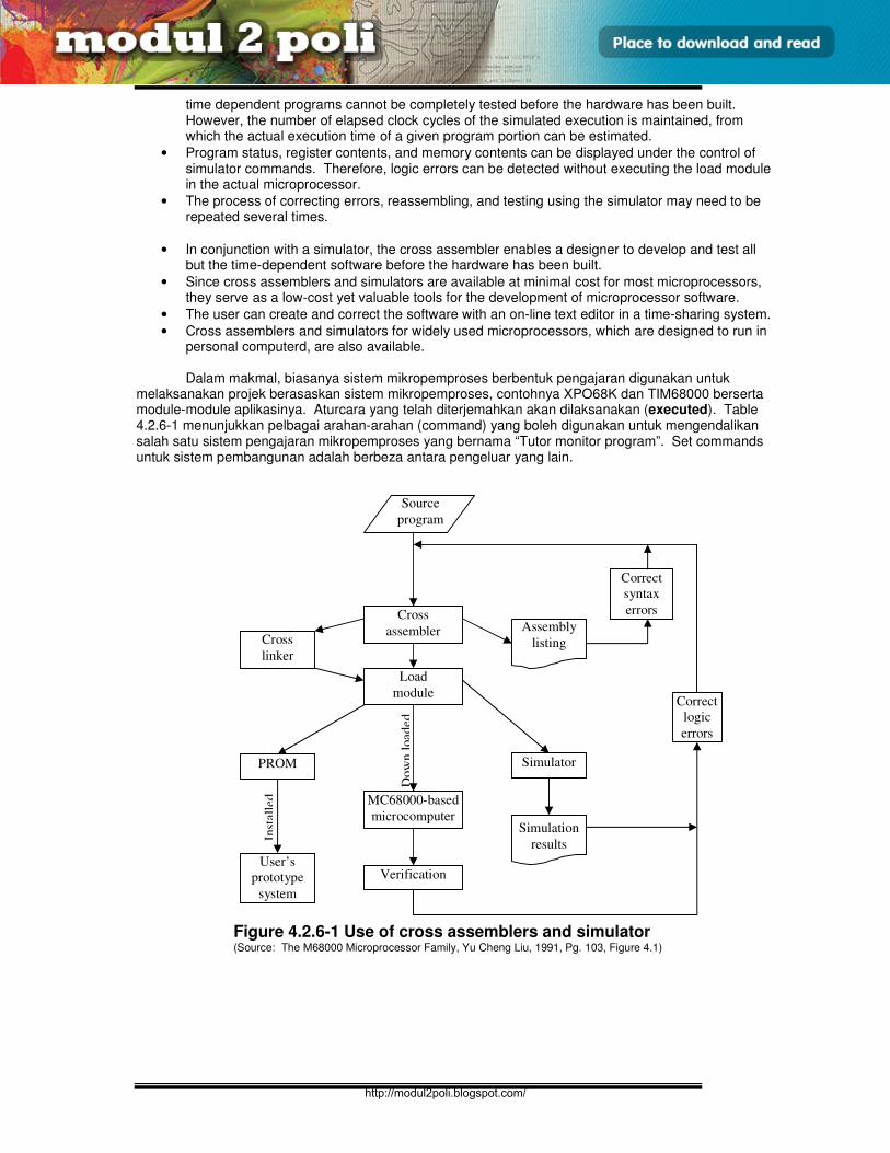
E3165 / UNIT 4 / 19
MOD PENGALAMATAN DAN PENGATURCARAAN
time dependent programs cannot be completely tested before the hardware has been built. However, the number of elapsed clock cycles of the simulated execution is maintained, from which the actual execution time of a given program portion can be estimated.
• Program status, register contents, and memory contents can be displayed under the control of simulator commands. Therefore, logic errors can be detected without executing the load module in the actual microprocessor.
• The process of correcting errors, reassembling, and testing using the simulator may need to be repeated several times.
• In conjunction with a simulator, the cross assembler enables a designer to develop and test all but the time-dependent software before the hardware has been built.
• Since cross assemblers and simulators are available at minimal cost for most microprocessors, they serve as a low-cost yet valuable tools for the development of microprocessor software.
• The user can create and correct the software with an on-line text editor in a time-sharing system.
• Cross assemblers and simulators for widely used microprocessors, which are designed to run in personal computerd, are also available.
Dalam makmal, biasanya sistem mikropemproses berbentuk pengajaran digunakan untuk melaksanakan projek berasaskan sistem mikropemproses, contohnya XPO68K dan TIM68000 berserta module-module aplikasinya. Aturcara yang telah diterjemahkan akan dilaksanakan (executed). Table 4.2.6-1 menunjukkan pelbagai arahan-arahan (command) yang boleh digunakan untuk mengendalikan salah satu sistem pengajaran mikropemproses yang bernama “Tutor monitor program”. Set commands untuk sistem pembangunan adalah berbeza antara pengeluar yang lain.
Figure 4.2.6-1 Use of cross assemblers and simulator (Source: The M68000 Microprocessor Family, Yu Cheng Liu, 1991, Pg. 103, Figure 4.1)
Cross
assembler
Load
module
MC68000-based
microcomputer
Verification
Cross
linker
PROM
User’s
prototype
system
Simulator
Simulation
results
Correct
syntax
errors
Correct
logic
errors
Source
program
Assembly
listing
Inst
alle
d
Dow
n l
oaded
http://modul2poli.blogspot.com/
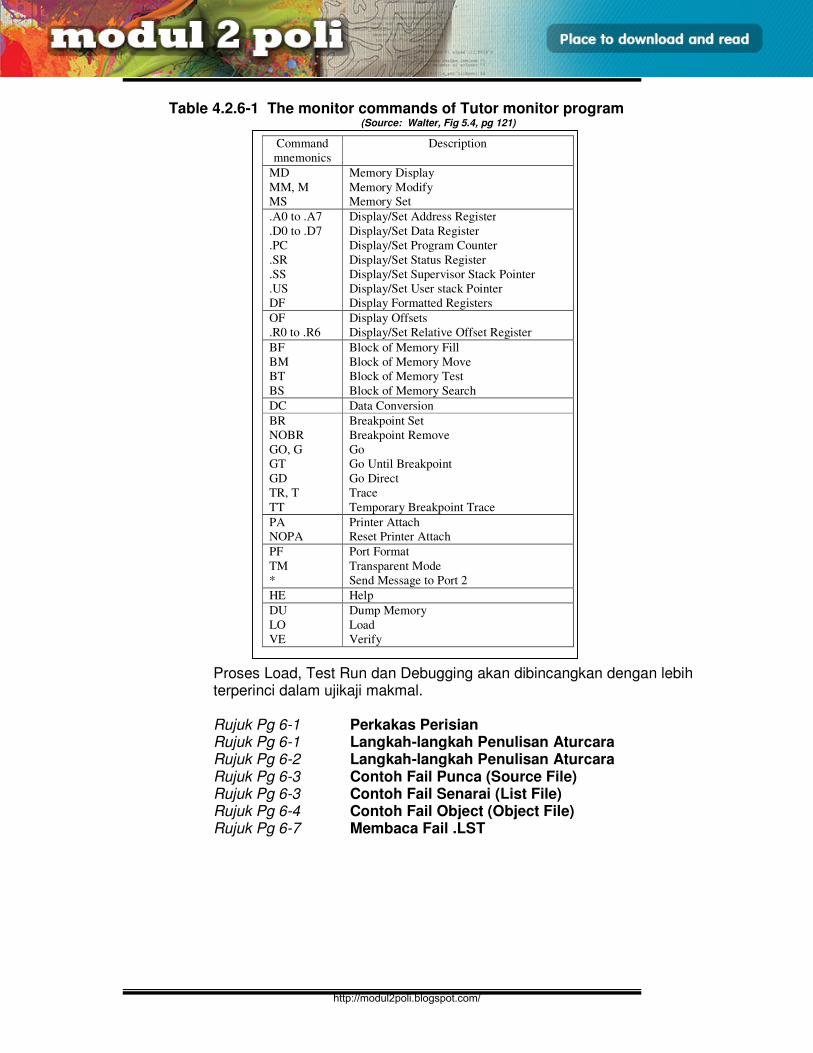
E3165 / UNIT 4 / 20
MOD PENGALAMATAN DAN PENGATURCARAAN
Table 4.2.6-1 The monitor commands of Tutor monitor program (Source: Walter, Fig 5.4, pg 121)
Proses Load, Test Run dan Debugging akan dibincangkan dengan lebih terperinci dalam ujikaji makmal. Rujuk Pg 6-1 Perkakas Perisian Rujuk Pg 6-1 Langkah-langkah Penulisan Aturcara Rujuk Pg 6-2 Langkah-langkah Penulisan Aturcara Rujuk Pg 6-3 Contoh Fail Punca (Source File) Rujuk Pg 6-3 Contoh Fail Senarai (List File) Rujuk Pg 6-4 Contoh Fail Object (Object File) Rujuk Pg 6-7 Membaca Fail .LST
Command
mnemonics
Description
MD
MM, M
MS
Memory Display
Memory Modify
Memory Set
.A0 to .A7
.D0 to .D7
.PC
.SR
.SS
.US
DF
Display/Set Address Register
Display/Set Data Register
Display/Set Program Counter
Display/Set Status Register
Display/Set Supervisor Stack Pointer
Display/Set User stack Pointer
Display Formatted Registers
OF
.R0 to .R6
Display Offsets
Display/Set Relative Offset Register
BF
BM
BT
BS
Block of Memory Fill
Block of Memory Move
Block of Memory Test
Block of Memory Search
DC Data Conversion
BR
NOBR
GO, G
GT
GD
TR, T
TT
Breakpoint Set
Breakpoint Remove
Go
Go Until Breakpoint
Go Direct
Trace
Temporary Breakpoint Trace
PA
NOPA
Printer Attach
Reset Printer Attach
PF
TM
*
Port Format
Transparent Mode
Send Message to Port 2
HE Help
DU
LO
VE
Dump Memory
Load
Verify
http://modul2poli.blogspot.com/
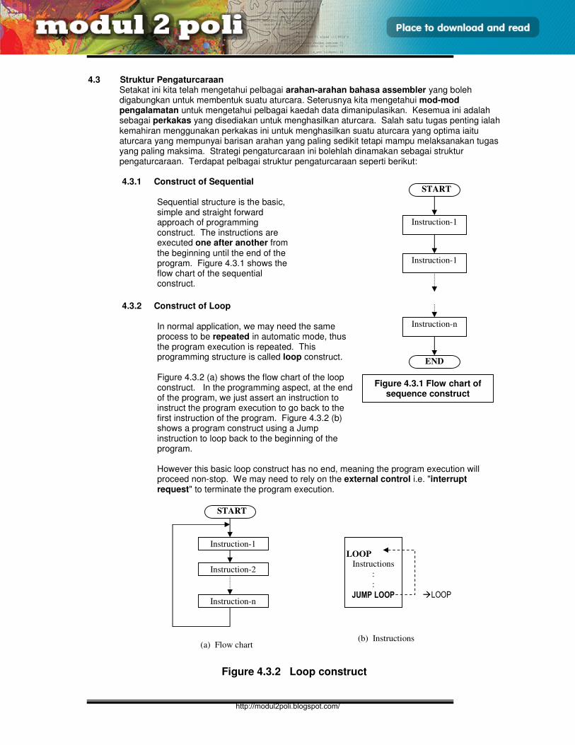
E3165 / UNIT 4 / 21
MOD PENGALAMATAN DAN PENGATURCARAAN
4.3 Struktur Pengaturcaraan
Setakat ini kita telah mengetahui pelbagai arahan-arahan bahasa assembler yang boleh digabungkan untuk membentuk suatu aturcara. Seterusnya kita mengetahui mod-mod pengalamatan untuk mengetahui pelbagai kaedah data dimanipulasikan. Kesemua ini adalah sebagai perkakas yang disediakan untuk menghasilkan aturcara. Salah satu tugas penting ialah kemahiran menggunakan perkakas ini untuk menghasilkan suatu aturcara yang optima iaitu aturcara yang mempunyai barisan arahan yang paling sedikit tetapi mampu melaksanakan tugas yang paling maksima. Strategi pengaturcaraan ini bolehlah dinamakan sebagai struktur pengaturcaraan. Terdapat pelbagai struktur pengaturcaraan seperti berikut:
4.3.1 Construct of Sequential
Sequential structure is the basic, simple and straight forward approach of programming construct. The instructions are executed one after another from the beginning until the end of the program. Figure 4.3.1 shows the flow chart of the sequential construct.
4.3.2 Construct of Loop
In normal application, we may need the same process to be repeated in automatic mode, thus the program execution is repeated. This programming structure is called loop construct. Figure 4.3.2 (a) shows the flow chart of the loop construct. In the programming aspect, at the end of the program, we just assert an instruction to instruct the program execution to go back to the first instruction of the program. Figure 4.3.2 (b) shows a program construct using a Jump instruction to loop back to the beginning of the program. However this basic loop construct has no end, meaning the program execution will proceed non-stop. We may need to rely on the external control i.e. "interrupt request" to terminate the program execution.
Figure 4.3.2 Loop construct
Instruction-1
(a) Flow chart
Instruction-2
Instruction-n
START
LOOP Instructions
:
:
JUMP LOOP LOOP
(b) Instructions
START
Instruction-1
END
Instruction-1
Instruction-n
Figure 4.3.1 Flow chart of sequence construct
http://modul2poli.blogspot.com/
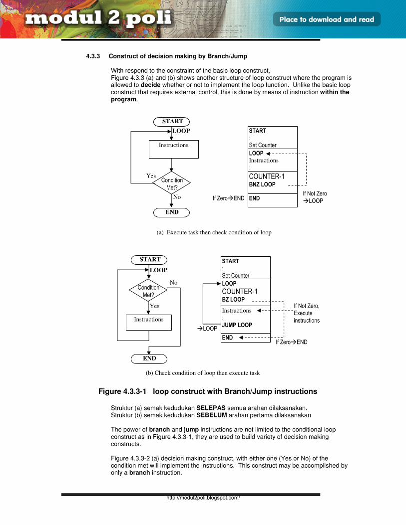
E3165 / UNIT 4 / 22
MOD PENGALAMATAN DAN PENGATURCARAAN
4.3.3 Construct of decision making by Branch/Jump
With respond to the constraint of the basic loop construct, Figure 4.3.3 (a) and (b) shows another structure of loop construct where the program is allowed to decide whether or not to implement the loop function. Unlike the basic loop construct that requires external control, this is done by means of instruction within the program.
Figure 4.3.3-1 loop construct with Branch/Jump instructions
Struktur (a) semak kedudukan SELEPAS semua arahan dilaksanakan. Struktur (b) semak kedudukan SEBELUM arahan pertama dilaksanakan
The power of branch and jump instructions are not limited to the conditional loop construct as in Figure 4.3.3-1, they are used to build variety of decision making constructs. Figure 4.3.3-2 (a) decision making construct, with either one (Yes or No) of the condition met will implement the instructions. This construct may be accomplished by only a branch instruction.
(a) Execute task then check condition of loop
(b) Check condition of loop then execute task
Instructions
Yes
No Condition
Met?
START
END
Instructions
:
JUMP LOOP
LOOP COUNTER-1 BZ LOOP
If ZeroEND
LOOP
END
START
: Set Counter
LOOP
If Not Zero, Execute
instructions
Instructions
Yes
No
START
END
LOOP Instructions
:
COUNTER-1 BNZ LOOP
If ZeroEND If Not Zero
LOOP END
START
: Set Counter
LOOP
Condition
Met?
http://modul2poli.blogspot.com/
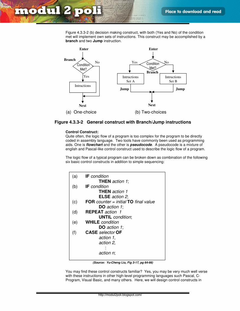
E3165 / UNIT 4 / 23
MOD PENGALAMATAN DAN PENGATURCARAAN
Figure 4.3.3-2 (b) decision making construct, with both (Yes and No) of the condition met will implement own sets of instructions. This construct may be accomplished by a branch and two Jump instruction.
(a) One-choice (b) Two-choices
Figure 4.3.3-2 General construct with Branch/Jump instructions Control Construct: Quite often, the logic flow of a program is too complex for the program to be directly coded in assembly language. Two tools have commonly been used as programming aids. One is flowchart and the other is pseudocode. A pseudocode is a mixture of english and Pascal-like control construct used to describe the logic flow of a program. The logic flow of a typical program can be broken down as combination of the following six basic control constructs in addition to simple sequencing:
(Source: Yu-Cheng Liu, Fig 3-17, pg 64-66)
You may find these control constructs familiar? Yes, you may be very much well verse with these instructions in other high-level programming languages such Pascal, C-Program, Visual Basic, and many others. Here, we will design control constructs in
Condition
Met?
Intructions
Yes
No Branch
Enter
Next
Condition Met?
Intructions
Set A
Yes No
Intructions
Set B
Branch
Jump Jump
Enter
Next
(a) IF condition THEN action 1;
(b) IF condition THEN action 1 ELSE action 2;
(c) FOR counter = initial TO final value DO action 1;
(d) REPEAT action 1 UNTIL condition;
(e) WHILE condition DO action 1;
(f) CASE selector OF action 1, action 2, : action n;
http://modul2poli.blogspot.com/
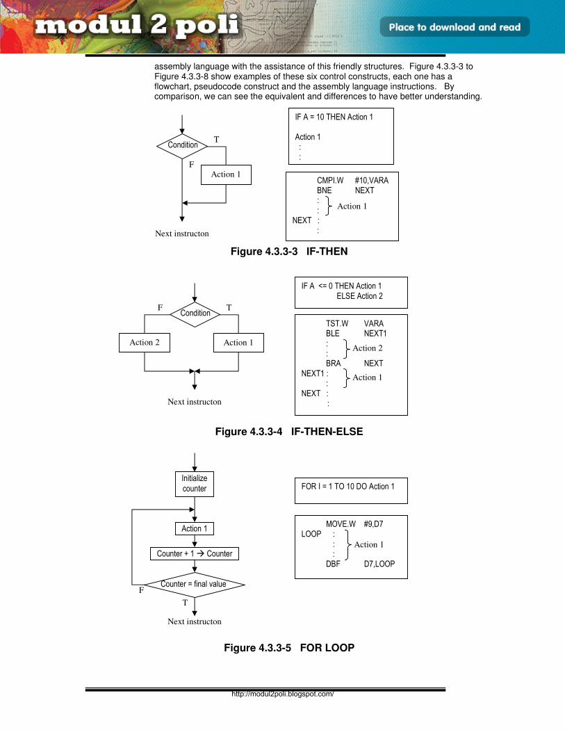
E3165 / UNIT 4 / 24
MOD PENGALAMATAN DAN PENGATURCARAAN
assembly language with the assistance of this friendly structures. Figure 4.3.3-3 to Figure 4.3.3-8 show examples of these six control constructs, each one has a flowchart, pseudocode construct and the assembly language instructions. By comparison, we can see the equivalent and differences to have better understanding.
Figure 4.3.3-3 IF-THEN
Figure 4.3.3-4 IF-THEN-ELSE
Figure 4.3.3-5 FOR LOOP
Condition
F
T
Next instructon
Action 1
IF A = 10 THEN Action 1 Action 1 : :
CMPI.W #10,VARA BNE NEXT : :
NEXT : :
Action 1
Condition
F T
Next instructon
Action 1
IF A <= 0 THEN Action 1 ELSE Action 2
TST.W VARA BLE NEXT1 : : BRA NEXT
NEXT1 : :
NEXT : :
Action 2 Action 2
Action 1
FOR I = 1 TO 10 DO Action 1
MOVE.W #9,D7 LOOP :
: : DBF D7,LOOP
Action 1
Counter = final value F
T
Next instructon
Counter + 1 Counter
Action 1
Initialize
counter
http://modul2poli.blogspot.com/
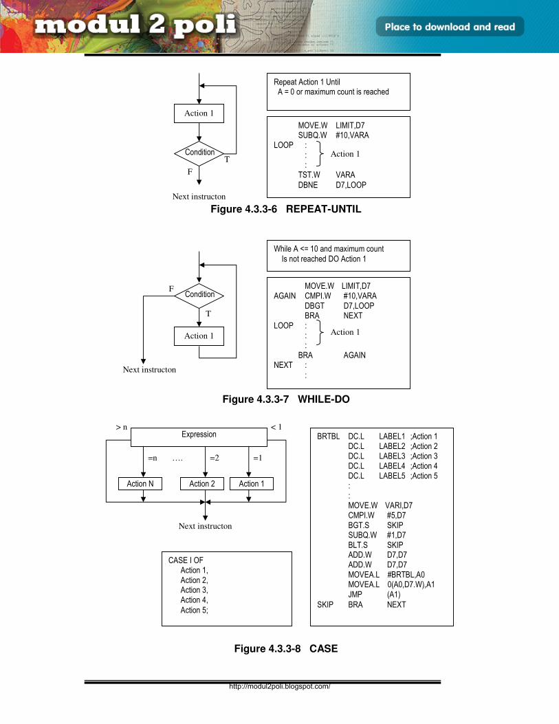
E3165 / UNIT 4 / 25
MOD PENGALAMATAN DAN PENGATURCARAAN
Figure 4.3.3-6 REPEAT-UNTIL
Figure 4.3.3-7 WHILE-DO
Figure 4.3.3-8 CASE
Condition
F
T
Next instructon
Action 1
Repeat Action 1 Until A = 0 or maximum count is reached
MOVE.W LIMIT,D7 SUBQ.W #10,VARA
LOOP : : :
TST.W VARA
DBNE D7,LOOP
Action 1
Condition
F
T
Next instructon
Action 1
While A <= 10 and maximum count
Is not reached DO Action 1
MOVE.W LIMIT,D7 AGAIN CMPI.W #10,VARA DBGT D7,LOOP BRA NEXT LOOP :
: :
BRA AGAIN NEXT :
:
Action 1
=1
Next instructon
Action 1
CASE I OF Action 1, Action 2, Action 3, Action 4,
Action 5;
BRTBL DC.L LABEL1 ;Action 1 DC.L LABEL2 ;Action 2 DC.L LABEL3 ;Action 3 DC.L LABEL4 ;Action 4 DC.L LABEL5 ;Action 5 : : MOVE.W VARI,D7
CMPI.W #5,D7 BGT.S SKIP
SUBQ.W #1,D7 BLT.S SKIP ADD.W D7,D7 ADD.W D7,D7 MOVEA.L #BRTBL,A0 MOVEA.L 0(A0,D7.W),A1 JMP (A1)
SKIP BRA NEXT
Action 2 Action N
Expression
=2 =n ….
< 1 > n
http://modul2poli.blogspot.com/
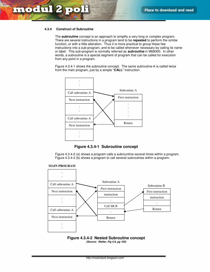
E3165 / UNIT 4 / 26
MOD PENGALAMATAN DAN PENGATURCARAAN
4.3.4 Construct of Subroutine
The subroutine concept is an approach to simplify a very long or complex program. There are several instructions in a program tend to be repeated to perform the similar function, or with a little alteration. Thus it is more practical to group these few instructions into a sub-program, and to be called whenever necessary by calling its name or label. This sub-program is normally referred as subroutine in M68000. In other words, a subroutine is a special segment of program that can be called for execution from any point in a program. Figure 4.3.4-1 shows the subroutine concept. The same subroutine-A is called twice from the main program, just by a simple "CALL" instruction.
Figure 4.3.4-2 (a) shows a program calls a subrountine several times within a program. Figure 4.3.4-2 (b) shows a program to call several subroutines within a program.
:
:
Call subroutine A
Next instruction
:
:
Call subroutine A
Next instruction
:
:
First instruction
Return
:
:
:
:
Subroutine A
Figure 4.3.4-1 Subroutine concept
Figure 4.3.4-2 Nested Subroutine concept (Source: Walter, Fig 4.9, pg 103)
:
:
Call subroutine A
Next instruction
:
:
Call subroutine A
Next instruction
:
:
First instruction
Subroutine A
instruction
:
Return
Call SR B
:
First instruction
instruction
:
Return
Subroutine B
MAIN PROGRAM
http://modul2poli.blogspot.com/
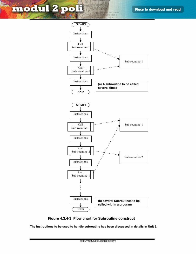
E3165 / UNIT 4 / 27
MOD PENGALAMATAN DAN PENGATURCARAAN
The instructions to be used to handle subroutine has been discussed in details in Unit 3.
END
START
Instructions
Call
Sub-rountine-1
Instructions
Call
Sub-rountine-1
Instructions
Sub-rountine-1
END
START
Instructions
Call
Sub-rountine-1
Instructions
Call
Sub-rountine-2
Instructions
Sub-rountine-1
Sub-rountine-2
Instructions
Call
Sub-rountine-1
(a) A subroutine to be called several times
Figure 4.3.4-3 Flow chart for Subroutine construct
(b) several Subroutines to be called within a program
http://modul2poli.blogspot.com/
E3165 / UNIT 5 / 1
SISTEM INGATAN
Objektif Am:
To know and understand the memory system.
Objektif Khusus:
At the end of the unit you should be able to:
5.1 explain the function and type of memory in computer system. 5.2 discuss and calculate the cells of memory. 5.3 classify and explain RAM and ROM 5.4 explain the design of decoder circuit 5.5 identify the pins configuration of RAM
UNIT 5
OBJEKTIF
http://modul2poli.blogspot.com/
E3165 / UNIT 5 / 2
SISTEM INGATAN
5.0 PENGENALAN KEPADA SISTEM INGATAN
Do you remember? …. what you have taken for dinner last night, where you took your lunch last Monday, who invented aeroplane, and so much other informations in your mind. All these informations are always referred to memory which is stored in your mind or brain. Similarly computer system consists of memory to store information in various forms and purposes such as control informations, program instructions, data, and temporary storage, and other informations to assist the implementation of computer system operation. The latest computer systems are digital system. The major advantage of digital over analog is the ability to easily store large quantities of digital information and data for short or long periods. This memory capability makes digital system so versatile and adaptable in many situations. For example, in a digital computer the internal main memory stores instruction that tell the computer what to do under all possible circumstances so that the computer will do its job with a minimum amount of human intervention. This chapter explains about a study on the most commonly used type of memory devices.
5.1 Fungsi dan jenis ingatan dalam sistem komputer
Where do we store our information or programs in a computer system? Your answer is probably harddisk, floppy disk, or CD–ROM. Correct, these are the secondary memory. There are two catagories of memory in a computer system, i.e. primary and secondary memory.
Primary memory is used as the internal memory of a computer, which is in constant communication with the process of a computer system.
Any program or data used by the program reside in the internel memory while the computer is working on that program. RAM and ROM ( to be define shortly) make up internel memory. Primary memory is also called internal memory, main memory, working memory, and semiconductive memory. RAM and ROM are semiconductor chips that provide fast operation. Primary (semiconductor) memory provides smaller capacity limited by the size and technology of semiconductor chips.
INPUT-5A
http://modul2poli.blogspot.com/
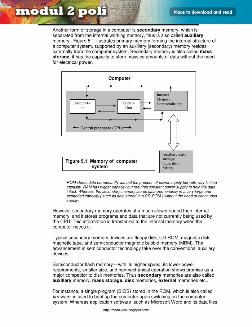
E3165 / UNIT 5 / 3
SISTEM INGATAN
Another form of storage in a computer is secondary memory, which is separated from the internal working memory, thus is also called auxiliary memory. Figure 5.1 illustrates primary memory forming the internal structure of a computer system, supported by an auxiliary (secondary) memory resides externally from the computer system. Secondary memory is also called mass storage, it has the capacity to store massive amounts of data without the need for electrical power. Computer Central processor (CPU)
ROM stores data permenantly without the present of power supply but with very limited capasity. RAM has bigger capacity but requires constant power supply to hold the data intact. Whereas the secondary memory stores data permenantly in a very large and expanded capacity ( such as data stored in a CD-ROM ) without the need of continuous supply.
However secondary memory operates at a much slower speed than internal memory, and it stores programs and data that are not currently being used by the CPU. This information is transferred to the internal memory when the computer needs it. Typical secondary memory devices are floppy disk, CD-ROM, magnetic disk, magnetic tape, and semiconductor magnetic bubble memory (MBM). The advancement in semiconductor technology take over the conventional auxiliary devices. Semiconductor flash memory – with its higher speed, its lower power requirements, smaller size, and nonmechanical operation shows promise as a major competitor to disk memories. Thus secondary memories are also called auxillary memory, mass storage, disk memories, external memories etc..
For instance, a single program (BIOS) stored in the ROM, which is also called firmware is used to boot up the computer upon switching on the computer system. Whereas application software such as Microsoft Word and its data files
Arithmetic
unit
Control
Unit
Internal
Memory
(semiconductor)
Auxiliary mass
strorage
(tape, disk,
MBM)
Figure 5.1 Memory of computer system
http://modul2poli.blogspot.com/
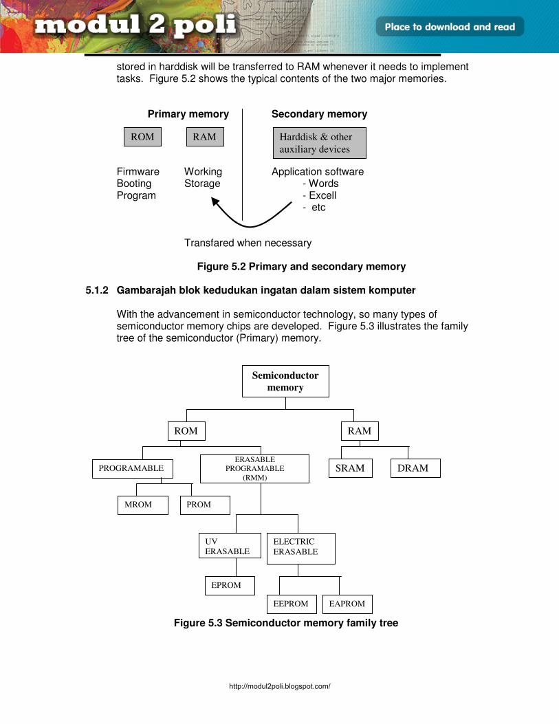
E3165 / UNIT 5 / 4
SISTEM INGATAN
stored in harddisk will be transferred to RAM whenever it needs to implement tasks. Figure 5.2 shows the typical contents of the two major memories.
Primary memory Secondary memory
Firmware Working Application software Booting Storage - Words Program - Excell
- etc Transfared when necessary
Figure 5.2 Primary and secondary memory
5.1.2 Gambarajah blok kedudukan ingatan dalam sistem komputer
With the advancement in semiconductor technology, so many types of semiconductor memory chips are developed. Figure 5.3 illustrates the family tree of the semiconductor (Primary) memory.
Figure 5.3 Semiconductor memory family tree
ROM RAM Harddisk & other
auxiliary devices
Semiconductor
memory
ROM RAM
SRAM DRAM PROGRAMABLE
MROM PROM
UV
ERASABLE
ELECTRIC
ERASABLE
EPROM
EEPROM EAPROM
ERASABLE
PROGRAMABLE
(RMM)
http://modul2poli.blogspot.com/
E3165 / UNIT 5 / 5
SISTEM INGATAN
5.1.3 ROM – Read Only Memory
• Ingatan jenis tak meruap (volatile), data tidak boleh diubah.
• Ingatan Baca sahaja. Kandungan ingatan yang boleh dibaca sahaja dan tidak boleh ditulis.
• Ingatan storan kekal,digunakan untuk menyimpan maklumat kekal seperti aturcara permulaan, program paparan, latarbelakang sistem komputer kesemuanya ini selalunya disebut perkukuhan (firmware - aturcara yang disimpan dalam ingatan kekal).
• Diaturcara oleh pegeluar mengikut spesifikasi pengguna. Maklumat ditulis ke dalam ROM sekali semasa pembuatan.
• Diaturcara menggunakan teknologi ‘photo-mask’.
• Data kekal selama-lamanya walaupun bekalan kuasa komputer diputuskan dan tidak boleh dipadam atau diubah.
• Dihasilkan dalam kuantiti yang banyak disebabkan masa yang panjang dan kosnya tinggi.
• Lokasi ingatan dipilih semasa pembuatan dan selepas itu ditetapkan.
• ROM terdiri daripada : i. Programmable (MROM/ PROM) ii. Erasable Programmable / Read Mostly Memories (RMM)
(EPROM/EEPROM/EAPROM) 5.1.3.1 Cabang Programmable ROM (PROM)
• ROM yang hanya boleh ditulis (diprogram) semasa proses pembuatan atau kali pertama oleh pengguna, selepas itu hanya untuk dibaca sahaja dan tidak dilakukan proses memadam dan memprogram semula.
• Contohnya: MROM/ PROM 5.1.3.2 Cabang Erasable Programmable ROM (EPROM) / Read Mostly Memory
(RMM)
• ROM yang boleh dipadamkan dan diprogramkan semula oleh pengguna.
• Seperti juga dengan ROM yang lain, fungsi utama ROM ini ialah untuk proses baca sahaja, namun demikian proses padam dan program semula dibenarkan.
• Contoh: EPROM/EEPROM/EAPROM)
• RMM boleh ditulis lebih dari sekali, tetapi operasi TULIS lebih rumit daripada operasi BACA oleh itu operasi TULIS jarang dilakukan (WRITE less, READ more). Dengan kata lain, data boleh dipadam dan diprogram semula. Oleh itu nama RMM dan Erasable Programmable ROM selalu dirujuk silang.
5.1.3.3 MROM
MROM iaitu ROM bertopeng (Masked ROM). MROM selalunya dirujuk sebagai ROM sahaja. MROM diaturcara secara tetap pada masa pengilangan mengikut spesifikasi
pengguna. Proses pengaturcaraannya menggunakan ‘photographic negative’ yang disebut
topeng (mask), untuk menyambung atau memutuskan link-link yang kepada litar diod atau transistor.
Oleh kerana topeng ini adalah mahal, jenis ROM ini hanya kos-ekonomi jika kuantiti pembuatan komponen yang lebih besar.
http://modul2poli.blogspot.com/
E3165 / UNIT 5 / 6
SISTEM INGATAN
Komputer akan menghasilkan topeng (masked) untuk litar terkamil ROM mengikut jadual kebenaran yang dikehendaki.
5.1.3.4 PROM
PROM ialah Programmable ROM PROM ialah ROM yang boleh diaturcara dengan menggunakan suatu jenis
peranti khas dipanggil pengaturcaraan PROM (PROM writer atau PROM burner).
Pengaturcaraan PROM dilakukan dengan memasukkan cip PROM ke dalam PROM programmer. Setiap bit dalamnya disimpan dengan fius-fius yang boleh diputuskan atau dikekalkan untuk mewakili dua keadaan logik-0 atau logik-1.
PROM tidak boleh digunakan lagi jika terdapat sebarang kesilapan pengaturcaraan.
5.1.3.5 EPROM
• Kaedah pengaturcaraannya sama seperti PROM iaitu menggunakan PROM Programmer.
• Tetapi kandungan EPROM boleh dipadamkan dengan meletakkan serpihan (chip) tersebut di bawah sinar ultra violet (UV). Oleh itu EPROM juga dipanggil UV-EPROM (Ultra-violet PROM).
• Serpihan ingatan ini boleh diaturcara semula.
• Harganya mahal, lebih kurang dua kali lebih tinggi dari PROM.
5.1.3.6 EAPROM (Electrically Alterable PROM)
• EAPROM tidak memerlukan keseluruhan serpihan (cip) untuk dipadamkan, tetapi membenarkan perubahan data pada lokasi yang ditentukan oleh pengguna.
• Proses memadamkan dan memprogram semula dilakukan pada papan litar tanpa mengeluarkan serpihan daripada papan litar.
• Proses ini mengaambil masa beberapa ms ke beberapa saat.
• Proses perubahan data dilakukan dengan mengenakan denyut elektrik kepada serpihan EAPROM.
5.1.3.7 EEPROM (Electrically Erasable PROM)
• Boleh diaturcara semula tanpa menanggalkan serpihan daripada sistem komputer.
• Ingatan ini merupakan ROM yang boleh dipadamkan menggunakan denyutan elektrik.
• Pemadaman data secara elektrik terpaksa dibuat ke atas kesemua lokasi di dalam sesuatu EEPROM, sebelum ia boleh diprogram semula.
• Kelebihannya aturcara pengawas boleh diubah dengan mudah.
• Harganya agak mahal dan masa tulisannya jauh lebih panjang daripada masa baca.
http://modul2poli.blogspot.com/
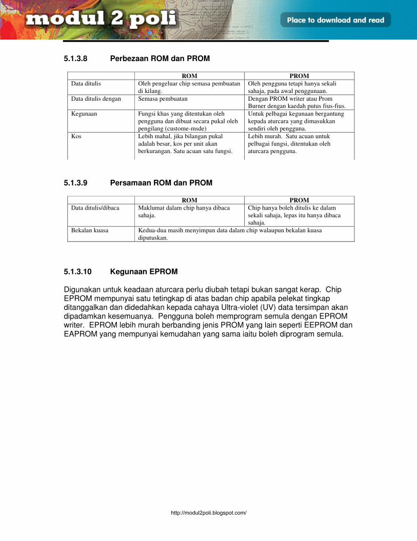
E3165 / UNIT 5 / 7
SISTEM INGATAN
5.1.3.8 Perbezaan ROM dan PROM 5.1.3.9 Persamaan ROM dan PROM 5.1.3.10 Kegunaan EPROM Digunakan untuk keadaan aturcara perlu diubah tetapi bukan sangat kerap. Chip EPROM mempunyai satu tetingkap di atas badan chip apabila pelekat tingkap ditanggalkan dan didedahkan kepada cahaya Ultra-violet (UV) data tersimpan akan dipadamkan kesemuanya. Pengguna boleh memprogram semula dengan EPROM writer. EPROM lebih murah berbanding jenis PROM yang lain seperti EEPROM dan EAPROM yang mempunyai kemudahan yang sama iaitu boleh diprogram semula.
ROM PROM
Data ditulis Oleh pengeluar chip semasa pembuatan
di kilang.
Oleh pengguna tetapi hanya sekali
sahaja, pada awal penggunaan.
Data ditulis dengan Semasa pembuatan Dengan PROM writer atau Prom
Burner dengan kaedah putus fius-fius.
Kegunaan Fungsi khas yang ditentukan oleh
pengguna dan dibuat secara pukal oleh
pengilang (custome-msde)
Untuk pelbagai kegunaan bergantung
kepada aturcara yang dimasukkan
sendiri oleh pengguna.
Kos Lebih mahal, jika bilangan pukal
adalah besar, kos per unit akan
berkurangan. Satu acuan satu fungsi.
Lebih murah. Satu acuan untuk
pelbagai fungsi, ditentukan oleh
aturcara pengguna.
ROM PROM
Data ditulis/dibaca Maklumat dalam chip hanya dibaca
sahaja.
Chip hanya boleh ditulis ke dalam
sekali sahaja, lepas itu hanya dibaca
sahaja.
Bekalan kuasa Kedua-dua masih menyimpan data dalam chip walaupun bekalan kuasa
diputuskan.
http://modul2poli.blogspot.com/
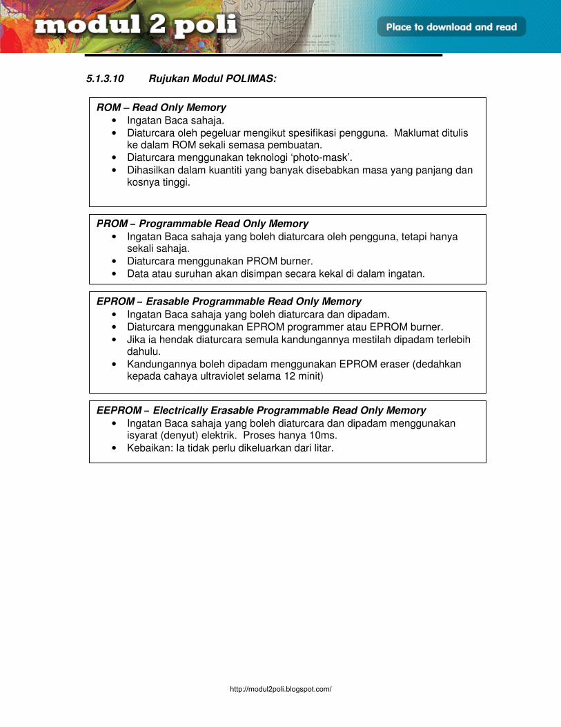
E3165 / UNIT 5 / 8
SISTEM INGATAN
5.1.3.10 Rujukan Modul POLIMAS:
ROM – Read Only Memory
• Ingatan Baca sahaja.
• Diaturcara oleh pegeluar mengikut spesifikasi pengguna. Maklumat ditulis ke dalam ROM sekali semasa pembuatan.
• Diaturcara menggunakan teknologi ‘photo-mask’.
• Dihasilkan dalam kuantiti yang banyak disebabkan masa yang panjang dan kosnya tinggi.
PROM – Programmable Read Only Memory
• Ingatan Baca sahaja yang boleh diaturcara oleh pengguna, tetapi hanya sekali sahaja.
• Diaturcara menggunakan PROM burner.
• Data atau suruhan akan disimpan secara kekal di dalam ingatan.
EPROM – Erasable Programmable Read Only Memory
• Ingatan Baca sahaja yang boleh diaturcara dan dipadam.
• Diaturcara menggunakan EPROM programmer atau EPROM burner.
• Jika ia hendak diaturcara semula kandungannya mestilah dipadam terlebih dahulu.
• Kandungannya boleh dipadam menggunakan EPROM eraser (dedahkan kepada cahaya ultraviolet selama 12 minit)
EEPROM – Electrically Erasable Programmable Read Only Memory
• Ingatan Baca sahaja yang boleh diaturcara dan dipadam menggunakan isyarat (denyut) elektrik. Proses hanya 10ms.
• Kebaikan: Ia tidak perlu dikeluarkan dari litar.
http://modul2poli.blogspot.com/
E3165 / UNIT 5 / 9
SISTEM INGATAN
5.1.4 RWM RWM – Read Write Memory ialah ingatan yang digunakan sebagai tempat simpanan sementara data untuk diproses di dalam sistem mikropemproses dan mikrokomputer. RWM juga dikenali sebagai RAM (Random Access Memory)
RAM – Random Access Memory
• RAM ialah ingatan jenis meruap (volatile), boleh diubah. Kandungannya boleh dibaca dan ditulis.
• Ingatan storan sementara, digunakan menyimpan maklumat sentiasa berubah-ubah semasa sistem beroperasi.
• Maklumat dalam ingatan terpadam bila bekalan kuasa komputer diputuskan dan hilang selama-lamanya kecuali jika maklumat disimpan dalam media simpanan kekal seperti suatu cakera.
• Biasanya digunakan bersama ingatan bantuan (sekunder) seperti ‘magnetic disk’ atan ‘dram storage’.
• Lokasi ingatannya boleh dicapai pada sebarang masa dan tempat tanpa mengikut turutan.
• RAM terdiri daripada : (i). SRAM (ii). DRAM 5.1.4.1 SRAM– Static RAM
Menggunakan flip-flop sebagai sel ingatan. Data tersimpan selagi bekalan kuasa dibekalkan kepada IC (ingatan meruap). Digunakan untuk sistem komputer berprestasi tinggi seperti Supercomputer
kerana kepantasan pemprosesan yang tinggi. Sejenis ingatan yang berkeupayaan untuk mengekalkan data yang disimpan di
dalamnya tanpa dipengaruhi oleh faktor masa. Guna kuasa yang tinggi. Ia keluarkan kuasa panas berlebihan bila digunakan
terlalu lama. 5.1.4.2 DRAM – Dynamic RAM
Menggunakan kapasitor sebagai sel ingatan. Data disimpan dalam bentuk bit sebagai cas-cas elektrik dalam kapasitor. Oleh itu ianya mesti disegar-semula (refresh) setiap beberapa ms bagi
mengekalkan datanya. Penggunaan kuasa yang rendah berbanding SRAM. Harga lebih murah.
5.1.4.3 Perbezaan dan operasi Ingatan statik dan dinamik
Ciri-ciri RAM DINAMIK (DRAM) RAM STATIK (SRAM)
Kerumitan sel ingatan lebih mudah/ringkas. lebih kompleks.
Saiz unit sel lebih kecil lebih besar
Bilangan sel ingatan per satu unit
kawasan.
lebih banyak sedikit
Bahan binaan kapasitor. flip-flop.
Memerlukan litar segaran Ya. untuk mengekalkan
kandungannya dalam kapasitor.
Tidak perlu.
Maklumat/data disimpan dalam
bentuk
Cas dalam kapasitor. Set atau reset flip-flop. Set=1 dan
Reset=0.
Kelajuan lebih perlahan. lebih pantas.
Kos/sel lebih murah. lebih mahal, terutama saiz ingatan
yang besar.
Penggunaan kuasa rendah. tinggi.
http://modul2poli.blogspot.com/

E3165 / UNIT 5 / 10
SISTEM INGATAN
5.1.4.4 Keperluan segar-semula (refreshing)
Litar segar-semula (refresh circuit) ialah satu litar tambahan yang dibina
berasaskan kapasitor yang boleh mengecas semula sel-sel ingatan dalam sebuah RAM Dinamik (DRAM).
Litar segar-semula digunakan dalam pembinan DRAM untuk pengecasan
semula sel-sel ingatan secara berkala, sekurang-kurangnya setiap 2 ms dan jika tidak, datanya akan hilang.
Data atau maklumat yang disimpan di dalam setiap unit sel bergantung kepada
ketumpatan cas pada pemuat. Cas yang penuh adalah logik-1, iaitu sel sedang menyimpan data 1, sementara logik-0 pula mewakili pemuat tidak menyimpan cas.
http://modul2poli.blogspot.com/
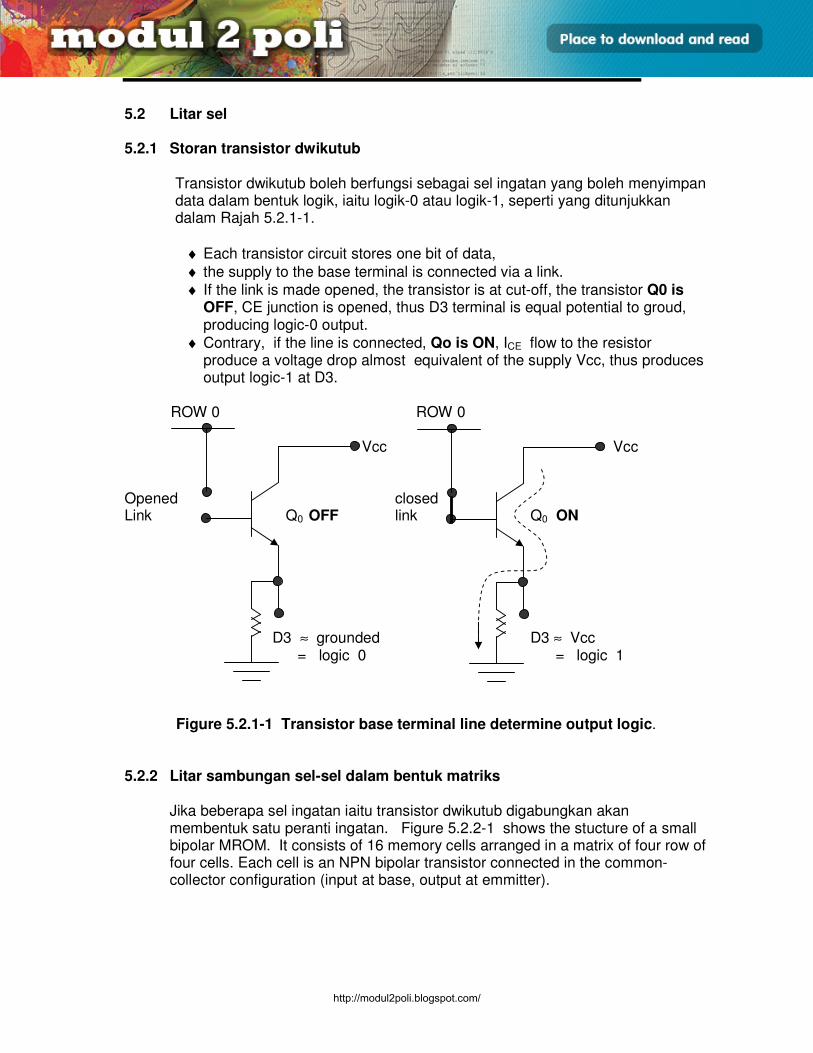
E3165 / UNIT 5 / 11
SISTEM INGATAN
5.2 Litar sel 5.2.1 Storan transistor dwikutub
Transistor dwikutub boleh berfungsi sebagai sel ingatan yang boleh menyimpan data dalam bentuk logik, iaitu logik-0 atau logik-1, seperti yang ditunjukkan dalam Rajah 5.2.1-1.
♦ Each transistor circuit stores one bit of data,
♦ the supply to the base terminal is connected via a link.
♦ If the link is made opened, the transistor is at cut-off, the transistor Q0 is OFF, CE junction is opened, thus D3 terminal is equal potential to groud, producing logic-0 output.
♦ Contrary, if the line is connected, Qo is ON, ICE flow to the resistor produce a voltage drop almost equivalent of the supply Vcc, thus produces output logic-1 at D3.
ROW 0 ROW 0
Vcc Vcc
Opened closed Link Q0 OFF link Q0 ON
D3 ≈ grounded D3 ≈ Vcc = logic 0 = logic 1
Figure 5.2.1-1 Transistor base terminal line determine output logic.
5.2.2 Litar sambungan sel-sel dalam bentuk matriks Jika beberapa sel ingatan iaitu transistor dwikutub digabungkan akan membentuk satu peranti ingatan. Figure 5.2.2-1 shows the stucture of a small bipolar MROM. It consists of 16 memory cells arranged in a matrix of four row of four cells. Each cell is an NPN bipolar transistor connected in the common-collector configuration (input at base, output at emmitter).
http://modul2poli.blogspot.com/
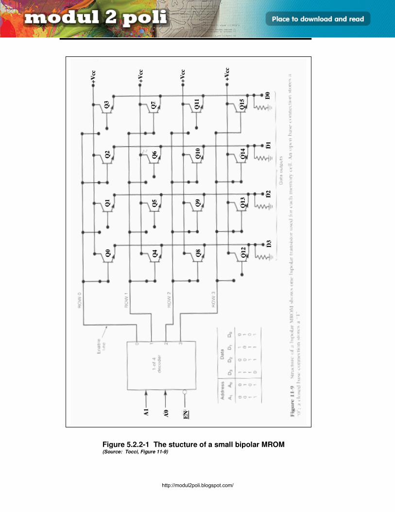
E3165 / UNIT 5 / 12
SISTEM INGATAN
Figure 5.2.2-1 The stucture of a small bipolar MROM (Source: Tocci, Figure 11-9)
Q3
Q2
Q1
Q0
Q7
Q6
Q5
Q4
Q11
Q
10
Q9
Q8
Q15
Q14
Q
13
Q
12
D0
D1
D
2
D3
+V
cc
+V
cc
+V
cc
+V
cc
A1
A0
EN
http://modul2poli.blogspot.com/
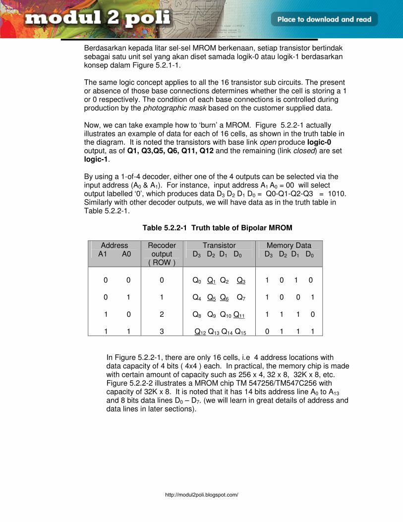
E3165 / UNIT 5 / 13
SISTEM INGATAN
Berdasarkan kepada litar sel-sel MROM berkenaan, setiap transistor bertindak sebagai satu unit sel yang akan diset samada logik-0 atau logik-1 berdasarkan konsep dalam Figure 5.2.1-1.
The same logic concept applies to all the 16 transistor sub circuits. The present or absence of those base connections determines whether the cell is storing a 1 or 0 respectively. The condition of each base connections is controlled during production by the photographic mask based on the customer supplied data. Now, we can take example how to ‘burn’ a MROM. Figure 5.2.2-1 actually illustrates an example of data for each of 16 cells, as shown in the truth table in the diagram. It is noted the transistors with base link open produce logic-0 output, as of Q1, Q3,Q5, Q6, Q11, Q12 and the remaining (link closed) are set logic-1. By using a 1-of-4 decoder, either one of the 4 outputs can be selected via the input address (A0 & A1). For instance, input address A1 A0 = 00 will select output labelled ‘0’, which produces data D3 D2 D1 D0 = Q0-Q1-Q2-Q3 = 1010. Similarly with other decoder outputs, we will have data as in the truth table in Table 5.2.2-1.
Table 5.2.2-1 Truth table of Bipolar MROM
Address A1 A0
Recoder output
( ROW )
Transistor D3 D2 D1 D0
Memory Data D3 D2 D1 D0
0 0 0 1
1 0 1 1
0
1
2
3
Q0 Q1 Q2 Q3 Q4 Q5 Q6 Q7 Q8 Q9 Q10 Q11 Q12 Q13 Q14 Q15
1 0 1 0 1 0 0 1 1 1 1 0 0 1 1 1
In Figure 5.2.2-1, there are only 16 cells, i.e 4 address locations with data capacity of 4 bits ( 4x4 ) each. In practical, the memory chip is made with certain amount of capacity such as 256 x 4, 32 x 8, 32K x 8, etc. Figure 5.2.2-2 illustrates a MROM chip TM 547256/TM547C256 with capacity of 32K x 8. It is noted that it has 14 bits address line A0 to A13 and 8 bits data lines D0 – D7. (we will learn in great details of address and data lines in later sections).
http://modul2poli.blogspot.com/
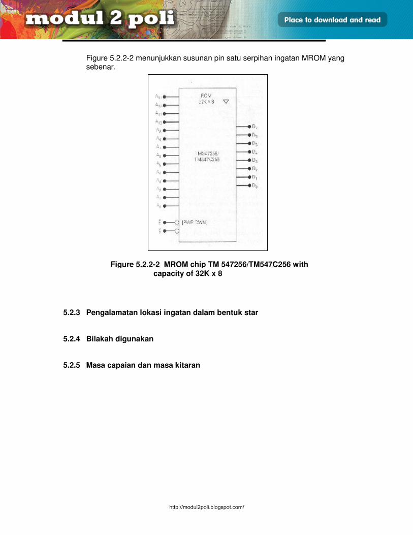
E3165 / UNIT 5 / 14
SISTEM INGATAN
Figure 5.2.2-2 menunjukkan susunan pin satu serpihan ingatan MROM yang sebenar.
5.2.3 Pengalamatan lokasi ingatan dalam bentuk star 5.2.4 Bilakah digunakan 5.2.5 Masa capaian dan masa kitaran
Figure 5.2.2-2 MROM chip TM 547256/TM547C256 with capacity of 32K x 8
http://modul2poli.blogspot.com/
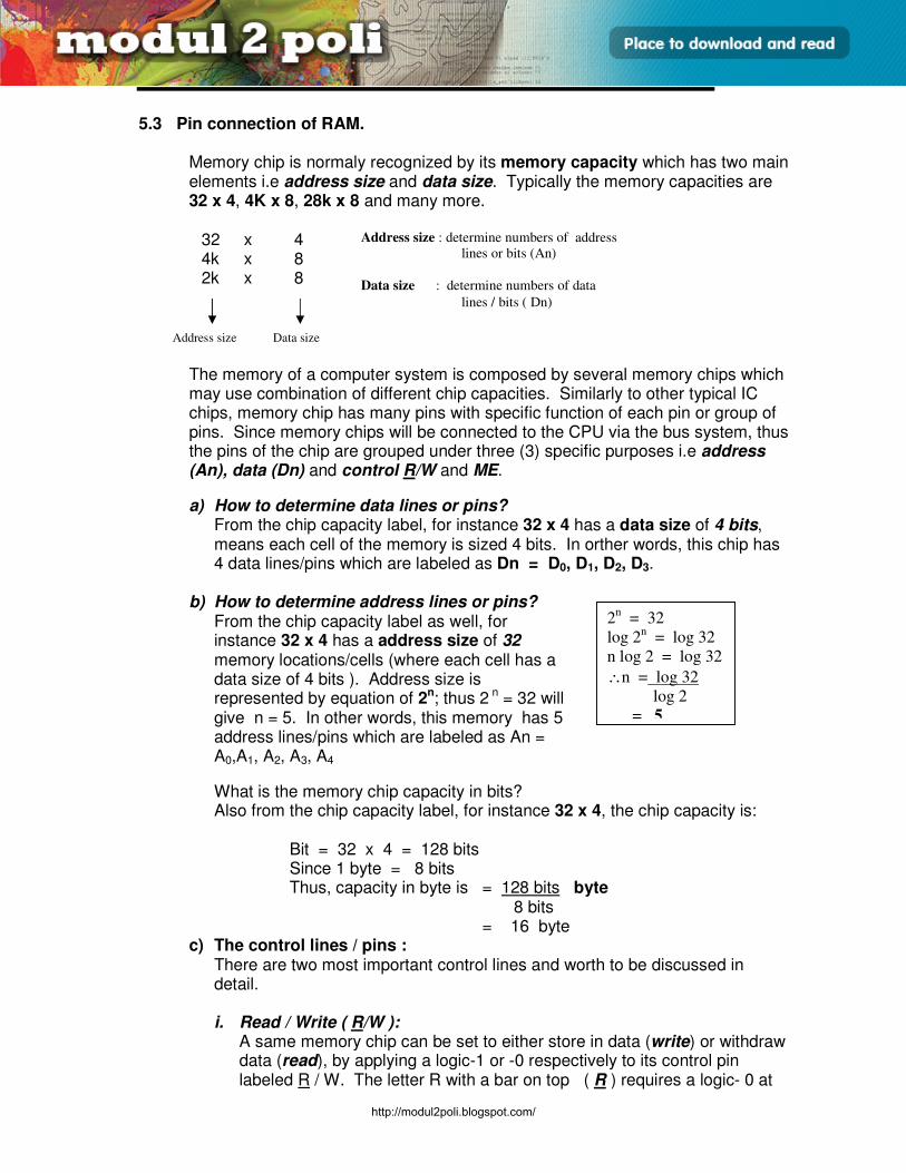
E3165 / UNIT 5 / 15
SISTEM INGATAN
5.3 Pin connection of RAM. Memory chip is normaly recognized by its memory capacity which has two main elements i.e address size and data size. Typically the memory capacities are 32 x 4, 4K x 8, 28k x 8 and many more.
32 x 4 4k x 8 2k x 8
The memory of a computer system is composed by several memory chips which may use combination of different chip capacities. Similarly to other typical IC chips, memory chip has many pins with specific function of each pin or group of pins. Since memory chips will be connected to the CPU via the bus system, thus the pins of the chip are grouped under three (3) specific purposes i.e address (An), data (Dn) and control R/W and ME.
a) How to determine data lines or pins? From the chip capacity label, for instance 32 x 4 has a data size of 4 bits, means each cell of the memory is sized 4 bits. In orther words, this chip has 4 data lines/pins which are labeled as Dn = D0, D1, D2, D3.
b) How to determine address lines or pins?
From the chip capacity label as well, for instance 32 x 4 has a address size of 32 memory locations/cells (where each cell has a data size of 4 bits ). Address size is represented by equation of 2n; thus 2 n = 32 will give n = 5. In other words, this memory has 5 address lines/pins which are labeled as An = A0,A1, A2, A3, A4
What is the memory chip capacity in bits? Also from the chip capacity label, for instance 32 x 4, the chip capacity is:
Bit = 32 x 4 = 128 bits Since 1 byte = 8 bits Thus, capacity in byte is = 128 bits byte 8 bits = 16 byte
c) The control lines / pins : There are two most important control lines and worth to be discussed in detail.
i. Read / Write ( R/W ):
A same memory chip can be set to either store in data (write) or withdraw data (read), by applying a logic-1 or -0 respectively to its control pin labeled R / W. The letter R with a bar on top ( R ) requires a logic- 0 at
Address size Data size
Address size : determine numbers of address
lines or bits (An)
Data size : determine numbers of data
lines / bits ( Dn)
2n = 32
log 2n = log 32
n log 2 = log 32
∴n = log 32
log 2
= 5
http://modul2poli.blogspot.com/
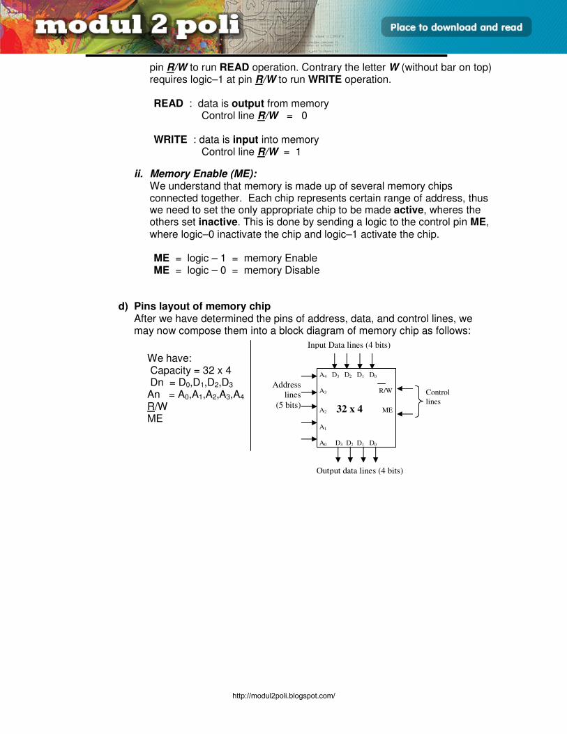
E3165 / UNIT 5 / 16
SISTEM INGATAN
pin R/W to run READ operation. Contrary the letter W (without bar on top) requires logic–1 at pin R/W to run WRITE operation.
READ : data is output from memory Control line R/W = 0 WRITE : data is input into memory Control line R/W = 1
ii. Memory Enable (ME): We understand that memory is made up of several memory chips connected together. Each chip represents certain range of address, thus we need to set the only appropriate chip to be made active, wheres the others set inactive. This is done by sending a logic to the control pin ME, where logic–0 inactivate the chip and logic–1 activate the chip.
ME = logic – 1 = memory Enable ME = logic – 0 = memory Disable
d) Pins layout of memory chip After we have determined the pins of address, data, and control lines, we may now compose them into a block diagram of memory chip as follows:
We have: Capacity = 32 x 4 Dn = D0,D1,D2,D3 An = A0,A1,A2,A3,A4
R/W ME
Output data lines (4 bits)
A4 D3 D2 D1 D0
A3 R/W
A2 32 x 4 ME
A1
A0 D3 D2 D1 D0
Address
lines
(5 bits)
Control
lines
Input Data lines (4 bits)
http://modul2poli.blogspot.com/
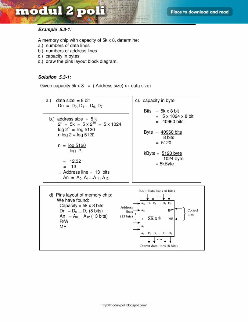
E3165 / UNIT 5 / 17
SISTEM INGATAN
Example 5.3-1: A memory chip with capacity of 5k x 8, determine: a.) numbers of data lines b.) numbers of address lines c.) capacity in bytes d.) draw the pins layout block diagram. Solution 5.3-1:
a.) data size = 8 bit Dn = D0, D1… D6, D7
b.) address size = 5 k 2n = 5k = 5 x 210 = 5 x 1024 log 2n = log 5120 n log 2 = log 5120
n = log 5120 log 2 = 12.32 = 13
∴ Address line = 13 bits An = A0, A1…A11, A12
c). capacity in byte Bits = 5k x 8 bit
= 5 x 1024 x 8 bit = 40960 bits
Byte = 40960 bits
8 bits = 5120
kByte = 5120 byte
1024 byte = 5kByte
d) Pins layout of memory chip: We have found:
Capacity = 5k x 8 bits Dn = D0 …. D7 (8 bits) An = A0 …..A12 (13 bits) R/W ME
Output data lines (8 bits)
A12 D7 D6 …. D1 D0
A11 R/W
: 5K x 8 ME
A1
A0 D7 D6 …. D1 D0
Address
lines
(13 bits)
Control
lines
Input Data lines (8 bits)
….
….
:
:
Given capacity 5k x 8 = ( Address size) x ( data size)
http://modul2poli.blogspot.com/
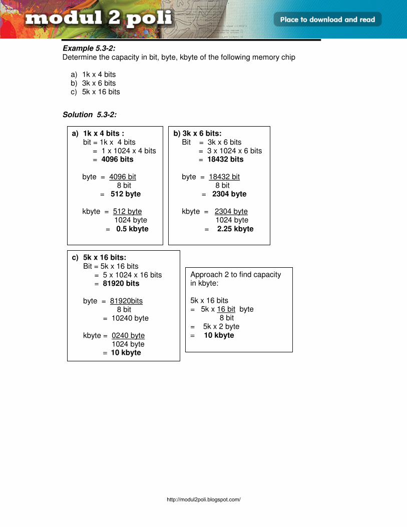
E3165 / UNIT 5 / 18
SISTEM INGATAN
Example 5.3-2: Determine the capacity in bit, byte, kbyte of the following memory chip
a) 1k x 4 bits b) 3k x 6 bits c) 5k x 16 bits
Solution 5.3-2:
b) 3k x 6 bits: Bit = 3k x 6 bits = 3 x 1024 x 6 bits = 18432 bits byte = 18432 bit 8 bit
= 2304 byte kbyte = 2304 byte 1024 byte
= 2.25 kbyte
a) 1k x 4 bits : bit = 1k x 4 bits
= 1 x 1024 x 4 bits = 4096 bits byte = 4096 bit 8 bit
= 512 byte kbyte = 512 byte
1024 byte = 0.5 kbyte
c) 5k x 16 bits: Bit = 5k x 16 bits
= 5 x 1024 x 16 bits = 81920 bits
byte = 81920bits
8 bit = 10240 byte
kbyte = 0240 byte
1024 byte = 10 kbyte
Approach 2 to find capacity in kbyte: 5k x 16 bits = 5k x 16 bit byte 8 bit = 5k x 2 byte = 10 kbyte
http://modul2poli.blogspot.com/
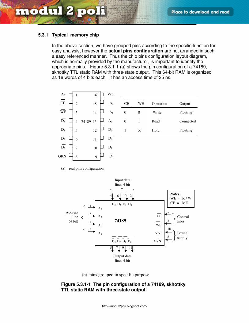
E3165 / UNIT 5 / 19
SISTEM INGATAN
5.3.1 Typical memory chip
In the above section, we have grouped pins according to the specific function for easy analysis, however the actual pins configuration are not arranged in such a easy referenced manner. Thus the chip pins configuration layout diagram, which is normally provided by the manufacturer, is important to identify the appropriate pins. Figure 5.3.1-1 (a) shows the pin configuration of a 74189, skhottky TTL static RAM with three-state output. This 64-bit RAM is organized as 16 words of 4 bits each. It has an access time of 35 ns.
CE WE Operation Output
0 0 Write Floating
0 1 Read Connected
1 X Hold Floating
A3 Vcc
CE A2
WE A1
D3 A0
D3 D0
D2 D0
D2 D1
GRN D1
1 16
2 15
3 14
4 74189 13
5 12
6 11
7 10
8 9
(a) real pins configuration
(b). pins grouped in specific purpose
Figure 5.3.1-1 The pin configuration of a 74189, skhottky TTL static RAM with three-state output.
Address
line
(4 bit)
D3 D2 D1 D0
A3
A2 CE
74189 A1 WE
A0 Vcc
_ _ _ _
D3 D2 D1 D0 GRN
Control
lines
Power
supply
Input data
lines 4 bit
4 6 10 12
5 7 9 11
2
3
16
8
1
15
14
13
Output data
lines 4 bit
Notes : WE = R / W
CE = ME
http://modul2poli.blogspot.com/
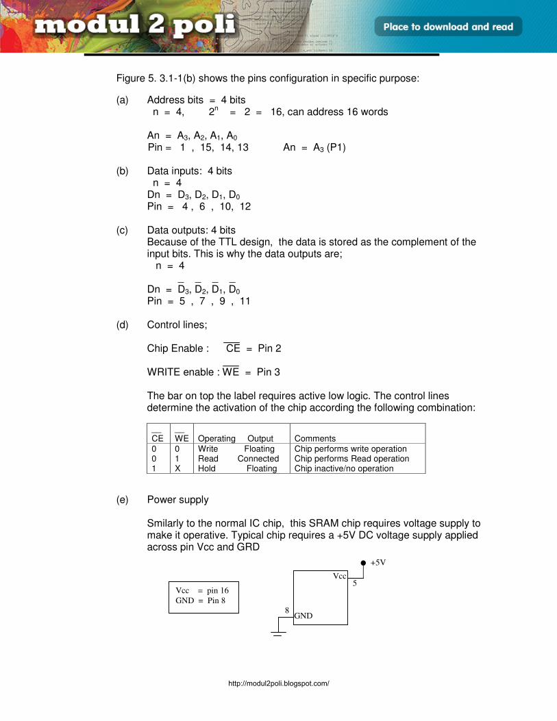
E3165 / UNIT 5 / 20
SISTEM INGATAN
Figure 5. 3.1-1(b) shows the pins configuration in specific purpose:
(a) Address bits = 4 bits n = 4, 2n = 2 = 16, can address 16 words An = A3, A2, A1, A0 Pin = 1 , 15, 14, 13 An = A3 (P1) (b) Data inputs: 4 bits n = 4 Dn = D3, D2, D1, D0 Pin = 4 , 6 , 10, 12 (c) Data outputs: 4 bits
Because of the TTL design, the data is stored as the complement of the input bits. This is why the data outputs are;
n = 4 _ _ _ _
Dn = D3, D2, D1, D0 Pin = 5 , 7 , 9 , 11 (d) Control lines;
Chip Enable : CE = Pin 2
WRITE enable : WE = Pin 3
The bar on top the label requires active low logic. The control lines determine the activation of the chip according the following combination:
__ CE
__ WE
Operating Output
Comments
0 0 1
0 1 X
Write Floating Read Connected Hold Floating
Chip performs write operation Chip performs Read operation Chip inactive/no operation
(e) Power supply
Smilarly to the normal IC chip, this SRAM chip requires voltage supply to make it operative. Typical chip requires a +5V DC voltage supply applied across pin Vcc and GRD
Vcc
GND
Vcc = pin 16
GND = Pin 8
5
8
+5V
http://modul2poli.blogspot.com/
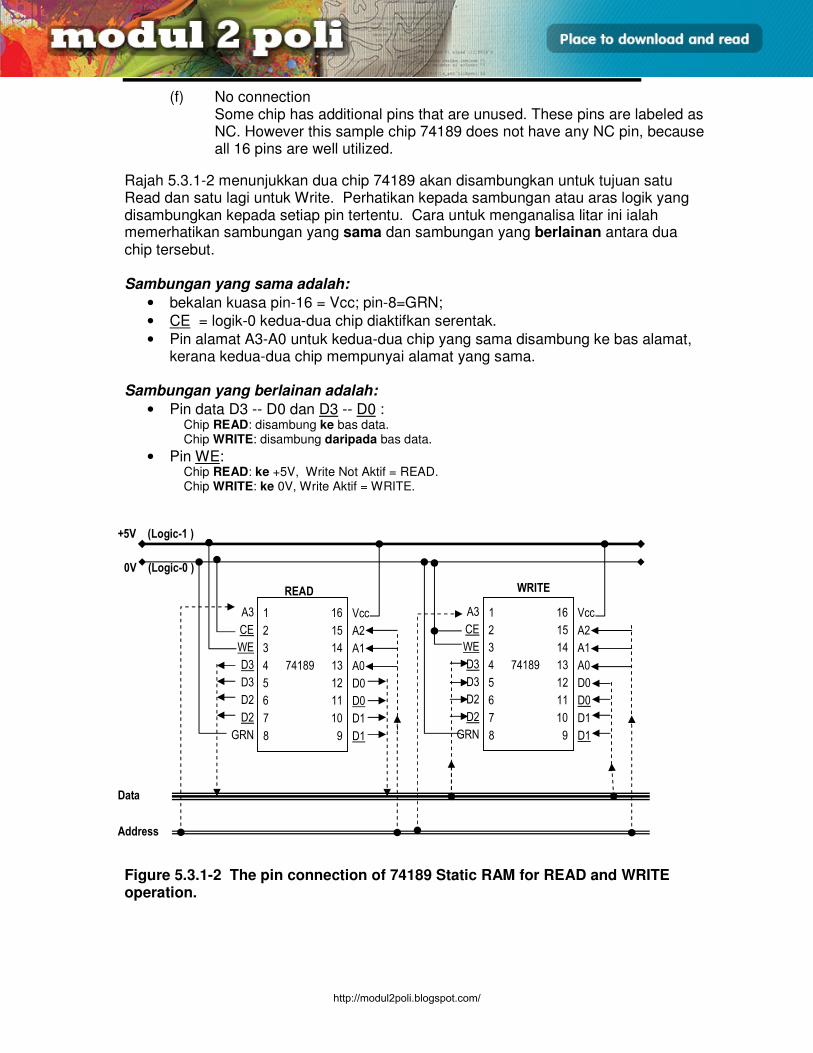
E3165 / UNIT 5 / 21
SISTEM INGATAN
(f) No connection Some chip has additional pins that are unused. These pins are labeled as NC. However this sample chip 74189 does not have any NC pin, because all 16 pins are well utilized.
Rajah 5.3.1-2 menunjukkan dua chip 74189 akan disambungkan untuk tujuan satu Read dan satu lagi untuk Write. Perhatikan kepada sambungan atau aras logik yang disambungkan kepada setiap pin tertentu. Cara untuk menganalisa litar ini ialah memerhatikan sambungan yang sama dan sambungan yang berlainan antara dua chip tersebut. Sambungan yang sama adalah:
• bekalan kuasa pin-16 = Vcc; pin-8=GRN;
• CE = logik-0 kedua-dua chip diaktifkan serentak.
• Pin alamat A3-A0 untuk kedua-dua chip yang sama disambung ke bas alamat, kerana kedua-dua chip mempunyai alamat yang sama.
Sambungan yang berlainan adalah:
• Pin data D3 -- D0 dan D3 -- D0 : Chip READ: disambung ke bas data. Chip WRITE: disambung daripada bas data.
• Pin WE: Chip READ: ke +5V, Write Not Aktif = READ. Chip WRITE: ke 0V, Write Aktif = WRITE.
Figure 5.3.1-2 The pin connection of 74189 Static RAM for READ and WRITE operation.
1 16
2 15
3 14
4 74189 13
5 12
6 11
7 10
8 9
A3
CE
WE
D3
D3
D2
D2
GRN
Vcc
A2
A1
A0
D0
D0
D1
D1
1 16
2 15
3 14
4 74189 13
5 12
6 11
7 10
8 9
A3
CE
WE
D3
D3
D2
D2
GRN
Vcc
A2
A1
A0
D0
D0
D1
D1
+5V (Logic-1 )
0V (Logic-0 )
READ WRITE
Address
Data
http://modul2poli.blogspot.com/
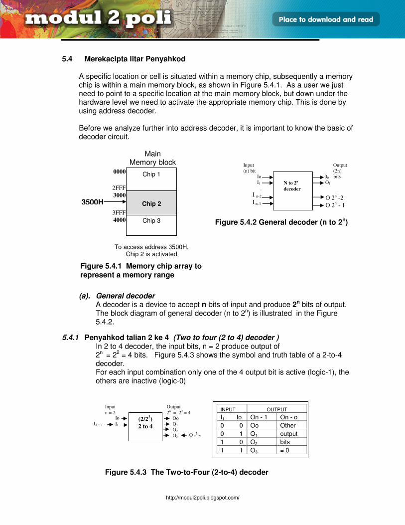
E3165 / UNIT 5 / 22
SISTEM INGATAN
5.4 Merekacipta litar Penyahkod
A specific location or cell is situated within a memory chip, subsequently a memory chip is within a main memory block, as shown in Figure 5.4.1. As a user we just need to point to a specific location at the main memory block, but down under the hardware level we need to activate the appropriate memory chip. This is done by using address decoder.
Before we analyze further into address decoder, it is important to know the basic of decoder circuit.
(a). General decoder A decoder is a device to accept n bits of input and produce 2n bits of output. The block diagram of general decoder (n to 2n) is illustrated in the Figure 5.4.2.
5.4.1 Penyahkod talian 2 ke 4 (Two to four (2 to 4) decoder ) In 2 to 4 decoder, the input bits, n = 2 produce output of 2n = 22 = 4 bits. Figure 5.4.3 shows the symbol and truth table of a 2-to-4 decoder. For each input combination only one of the 4 output bit is active (logic-1), the others are inactive (logic-0)
(2/22)
2 to 4
Io
I1 Oo
O1
O2
O3
Input
n = 2
Output
2n = 22 = 4
I2 - 1
O 22 -1
Input Output
(n) bit (2n) Io 00 bits
I1 O1
: n N to 2n
decoder
I n-2
I n-1 O 2n -2
O 2n - 1
Figure 5.4.2 General decoder (n to 2n)
INPUT OUTPUT
I1 Io On - 1 On - o
0 0 Oo Other
0 1 O1 output
1 0 O2 bits
1 1 O3 = 0
Main Memory block
3500H
0000
2FFF
3000
3FFF
4000
Chip 1
Chip 3
Chip 2
To access address 3500H, Chip 2 is activated
Figure 5.4.1 Memory chip array to represent a memory range
Figure 5.4.3 The Two-to-Four (2-to-4) decoder
http://modul2poli.blogspot.com/
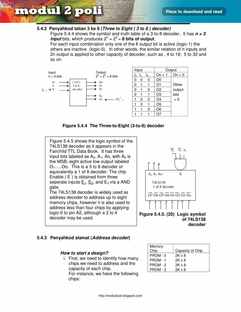
E3165 / UNIT 5 / 23
SISTEM INGATAN
5.4.2 Penyahkod talian 3 ke 8 (Three to Eight ( 3 to 8 ) decoder) Figure 5.4.4 shows the symbol and truth table of a 3-to-8 decoder. It has n = 3 input bits, which produces 2n = 23 = 8 bits of output. For each input combination only one of the 8 output bit is active (logic-1) the others are inactive (logic-0). In other words, the similar relation of n inputs and 2n output is applied to other capacity of decoder, such as , 4 to 16; 5 to 32 and so on.
5.4.3 Penyahkod alamat (Address decoder)
How to start a design? i. First, we need to identify how many
chips we need to address and the capacity of each chip. For instance, we have the following chips:
Memory Chip Capasity of Chip
PROM - 0 2K x 8
PROM - 1 2K x 8
PROM - 2 2K x 8
PROM - 3 2K x 8
Input Output
I2 I1 I0 On = 1 On = 0
0 0 0 O0
0 1 1 O1 Other
0 1 0 O2 output
0 1 1 O3 bits
1 0 0 O4 = 0
1 0 1 O5
1 1 0 O6
1 1 1 O7
Figure 5.4.4 The Three-to-Eight (3-to-8) decoder
( 3/23) 3 to 8
decoder
Io
I1
I2
Oo
O1
O2
:
O6
O7 O23 - 1
Output 2
n = 2
3 = 8 bits
Input n = 3 bits
I3 - 1
A2 A1 Ao E
74LS138
1 of 8 decoder
O7 O6 O5 O4 O3 O2 O1 Oo
o o o
o
o o o o
o o o
o
o
E1 E2 E3
Figure 5.4.5. (20) Logic symbol of 74LS138
decoder
Figure 5.4.5 shows the logic symbol of the 74LS138 decoder as it appears in the Fairchild TTL Data Book. It has three input bits labeled as A2, A1, Ao, with A2 is the MSB; eight active low output labeled O7…..Oo. This is a 3 to 8 decoder or equivalently a 1 of 8 decoder. The chip Enable ( E ) is obtained from three seperate inputs E1, E2, and E3 via a AND gate. The 74LS138 decoder is widely used as address decoder to address up to eight memory chips, however it is also used to address less than four chips by applying logic-0 to pin A2, although a 2 to 4 decoder may be used.
http://modul2poli.blogspot.com/
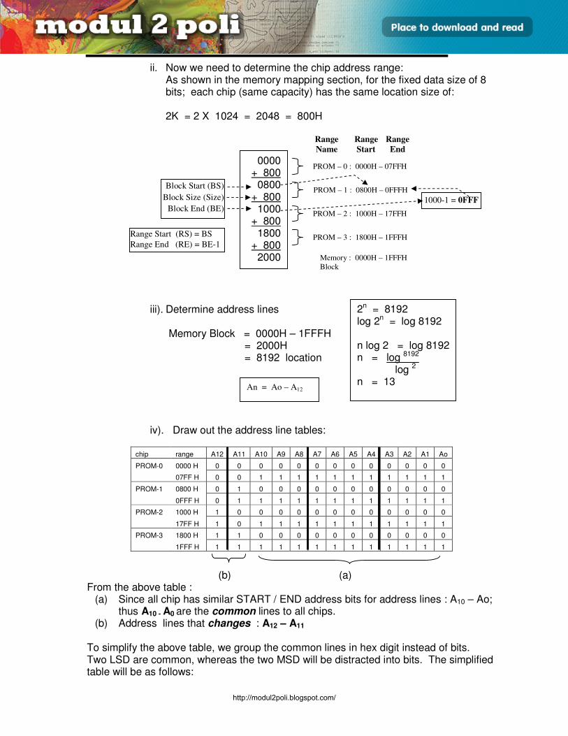
E3165 / UNIT 5 / 24
SISTEM INGATAN
ii. Now we need to determine the chip address range: As shown in the memory mapping section, for the fixed data size of 8 bits; each chip (same capacity) has the same location size of: 2K = 2 X 1024 = 2048 = 800H
iii). Determine address lines
Memory Block = 0000H – 1FFFH = 2000H = 8192 location
iv). Draw out the address line tables: (b) (a) From the above table :
(a) Since all chip has similar START / END address bits for address lines : A10 – Ao; thus A10 - A0 are the common lines to all chips.
(b) Address lines that changes : A12 – A11
To simplify the above table, we group the common lines in hex digit instead of bits. Two LSD are common, whereas the two MSD will be distracted into bits. The simplified table will be as follows:
An = Ao – A12
chip range A12 A11 A10 A9 A8 A7 A6 A5 A4 A3 A2 A1 Ao
PROM-0 0000 H 0 0 0 0 0 0 0 0 0 0 0 0 0
07FF H 0 0 1 1 1 1 1 1 1 1 1 1 1
PROM-1 0800 H 0 1 0 0 0 0 0 0 0 0 0 0 0
0FFF H 0 1 1 1 1 1 1 1 1 1 1 1 1
PROM-2 1000 H 1 0 0 0 0 0 0 0 0 0 0 0 0
17FF H 1 0 1 1 1 1 1 1 1 1 1 1 1
PROM-3 1800 H 1 1 0 0 0 0 0 0 0 0 0 0 0
1FFF H 1 1 1 1 1 1 1 1 1 1 1 1 1
Block Start (BS)
Block Size (Size)
Block End (BE)
Range Start (RS) = BS
Range End (RE) = BE-1
0000 + 800
0800 + 800
1000 + 800
1800 + 800
2000
PROM – 0 : 0000H – 07FFH
PROM – 1 : 0800H – 0FFFH
PROM – 2 : 1000H – 17FFH
PROM – 3 : 1800H – 1FFFH
1000-1 = 0FFF
Memory : 0000H – 1FFFH
Block
Range
Start
Range
End
Range
Name
2n = 8192 log 2n = log 8192 n log 2 = log 8192 n = log 8192 log 2 n = 13
http://modul2poli.blogspot.com/
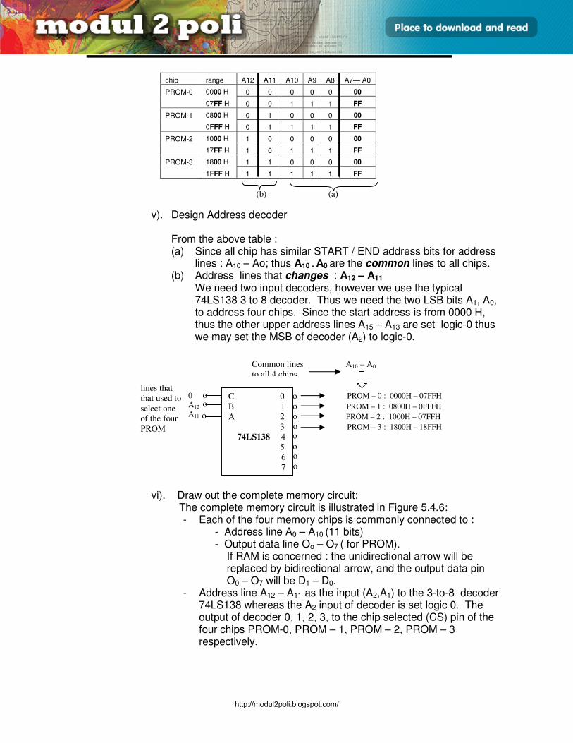
E3165 / UNIT 5 / 25
SISTEM INGATAN
v). Design Address decoder
From the above table : (a) Since all chip has similar START / END address bits for address
lines : A10 – Ao; thus A10 - A0 are the common lines to all chips. (b) Address lines that changes : A12 – A11
We need two input decoders, however we use the typical 74LS138 3 to 8 decoder. Thus we need the two LSB bits A1, A0, to address four chips. Since the start address is from 0000 H, thus the other upper address lines A15 – A13 are set logic-0 thus we may set the MSB of decoder (A2) to logic-0.
vi). Draw out the complete memory circuit:
The complete memory circuit is illustrated in Figure 5.4.6: - Each of the four memory chips is commonly connected to :
- Address line A0 – A10 (11 bits) - Output data line Oo – O7 ( for PROM).
If RAM is concerned : the unidirectional arrow will be replaced by bidirectional arrow, and the output data pin O0 – O7 will be D1 – D0.
- Address line A12 – A11 as the input (A2,A1) to the 3-to-8 decoder 74LS138 whereas the A2 input of decoder is set logic 0. The output of decoder 0, 1, 2, 3, to the chip selected (CS) pin of the four chips PROM-0, PROM – 1, PROM – 2, PROM – 3 respectively.
C 0
B 1
A 2
3
74LS138 4
5
6
7
o
o
o
o o
o
o
o
o
o
o PROM – 0 : 0000H – 07FFH
PROM – 1 : 0800H – 0FFFH
PROM – 2 : 1000H – 07FFH
PROM – 3 : 1800H – 18FFH
A10 – A0
0
A12
A11
Common lines
to all 4 chips
lines that
that used to
select one
of the four
PROM
chip range A12 A11 A10 A9 A8 A7— A0
PROM-0 0000 H 0 0 0 0 0 00
07FF H 0 0 1 1 1 FF
PROM-1 0800 H 0 1 0 0 0 00
0FFF H 0 1 1 1 1 FF
PROM-2 1000 H 1 0 0 0 0 00
17FF H 1 0 1 1 1 FF
PROM-3 1800 H 1 1 0 0 0 00
1FFF H 1 1 1 1 1 FF
(b) (a)
http://modul2poli.blogspot.com/
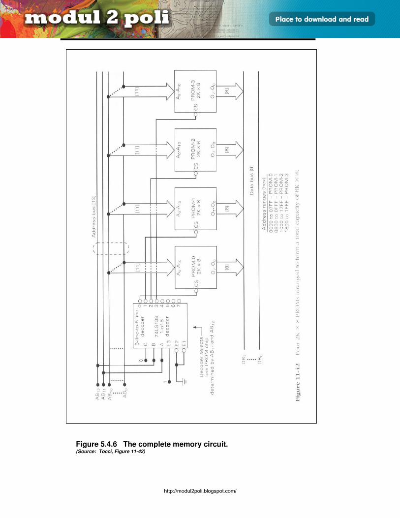
E3165 / UNIT 5 / 26
SISTEM INGATAN
Figure 5.4.6 The complete memory circuit. (Source: Tocci, Figure 11-42)
http://modul2poli.blogspot.com/
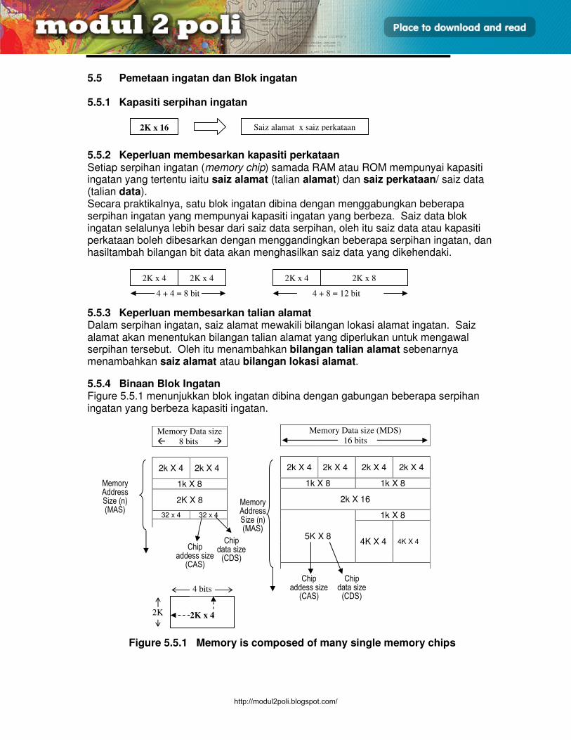
E3165 / UNIT 5 / 27
SISTEM INGATAN
5.5 Pemetaan ingatan dan Blok ingatan 5.5.1 Kapasiti serpihan ingatan
5.5.2 Keperluan membesarkan kapasiti perkataan Setiap serpihan ingatan (memory chip) samada RAM atau ROM mempunyai kapasiti ingatan yang tertentu iaitu saiz alamat (talian alamat) dan saiz perkataan/ saiz data (talian data). Secara praktikalnya, satu blok ingatan dibina dengan menggabungkan beberapa serpihan ingatan yang mempunyai kapasiti ingatan yang berbeza. Saiz data blok ingatan selalunya lebih besar dari saiz data serpihan, oleh itu saiz data atau kapasiti perkataan boleh dibesarkan dengan menggandingkan beberapa serpihan ingatan, dan hasiltambah bilangan bit data akan menghasilkan saiz data yang dikehendaki. 5.5.3 Keperluan membesarkan talian alamat Dalam serpihan ingatan, saiz alamat mewakili bilangan lokasi alamat ingatan. Saiz alamat akan menentukan bilangan talian alamat yang diperlukan untuk mengawal serpihan tersebut. Oleh itu menambahkan bilangan talian alamat sebenarnya menambahkan saiz alamat atau bilangan lokasi alamat.
5.5.4 Binaan Blok Ingatan Figure 5.5.1 menunjukkan blok ingatan dibina dengan gabungan beberapa serpihan ingatan yang berbeza kapasiti ingatan.
Figure 5.5.1 Memory is composed of many single memory chips
Chip addess size
(CAS)
Memory Address Size (n) (MAS)
Chip data size (CDS)
2K x 4
4 bits
2K
Memory data size
16 bit
2k X 4 2k X 4 2k X 4 2k X 4
1k X 8 1K X 8
2k X 16
5K X 8
1K X 8
4K X 4 4K X 4
Memory Data size (MDS)
16 bits
2k X 4 2k X 4 2k X 4 2k X 4
1k X 8 1k X 8
2k X 16
5K X 8
1k X 8
4K X 4 4K X 4
Memory Data size
8 bits
2k X 4 2k X 4
1k X 8
2K X 8
32 x 4 32 x 4
Memory Address Size (n) (MAS)
Chip addess size
(CAS)
Chip data size (CDS)
2K x 4 2K x 4
4 + 4 = 8 bit
2K x 4 2K x 8
4 + 8 = 12 bit
Saiz alamat x saiz perkataan 2K x 16
http://modul2poli.blogspot.com/
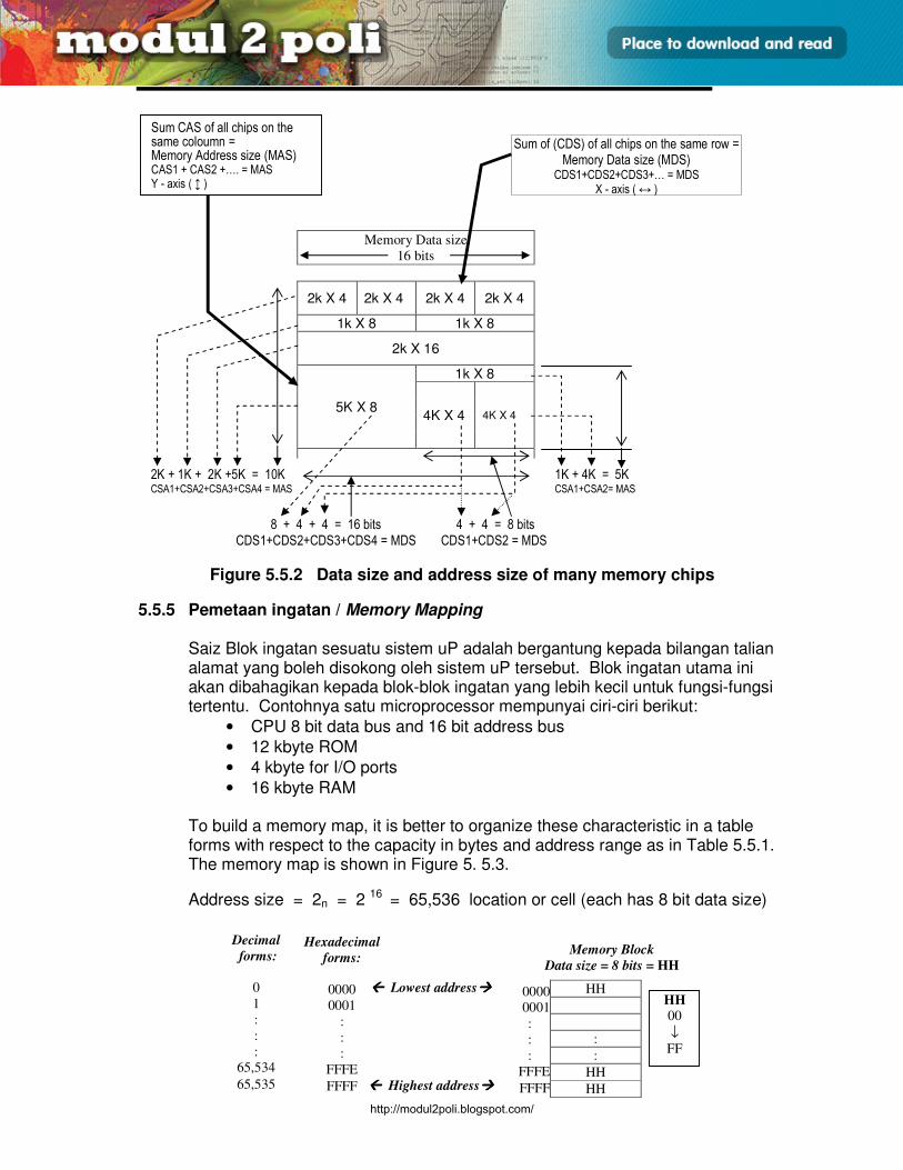
E3165 / UNIT 5 / 28
SISTEM INGATAN
Figure 5.5.2 Data size and address size of many memory chips
5.5.5 Pemetaan ingatan / Memory Mapping
Saiz Blok ingatan sesuatu sistem uP adalah bergantung kepada bilangan talian alamat yang boleh disokong oleh sistem uP tersebut. Blok ingatan utama ini akan dibahagikan kepada blok-blok ingatan yang lebih kecil untuk fungsi-fungsi tertentu. Contohnya satu microprocessor mempunyai ciri-ciri berikut:
• CPU 8 bit data bus and 16 bit address bus
• 12 kbyte ROM
• 4 kbyte for I/O ports
• 16 kbyte RAM To build a memory map, it is better to organize these characteristic in a table forms with respect to the capacity in bytes and address range as in Table 5.5.1. The memory map is shown in Figure 5. 5.3.
Address size = 2n = 2 16 = 65,536 location or cell (each has 8 bit data size)
Decimal
forms:
0
1
:
:
:
65,534
65,535
Hexadecimal
forms:
0000
0001
:
:
:
FFFE
FFFF
HH
:
:
HH
HH
0000
0001
:
:
:
FFFE
FFFF
Lowest address
Highest address
Memory Block
Data size = 8 bits = HH
HH
00
↓ FF
8 + 4 + 4 = 16 bits CDS1+CDS2+CDS3+CDS4 = MDS
Sum CAS of all chips on the same coloumn = Memory Address size (MAS) CAS1 + CAS2 +…. = MAS Y - axis ( )
Memory Data size
16 bits
2k X 4 2k X 4 2k X 4 2k X 4
1k X 8 1k X 8
2k X 16
5K X 8
1k X 8
4K X 4 4K X 4
2K + 1K + 2K +5K = 10K CSA1+CSA2+CSA3+CSA4 = MAS
1K + 4K = 5K CSA1+CSA2= MAS
Sum of (CDS) of all chips on the same row = Memory Data size (MDS)
CDS1+CDS2+CDS3+… = MDS X - axis ( ↔ )
4 + 4 = 8 bits CDS1+CDS2 = MDS
http://modul2poli.blogspot.com/
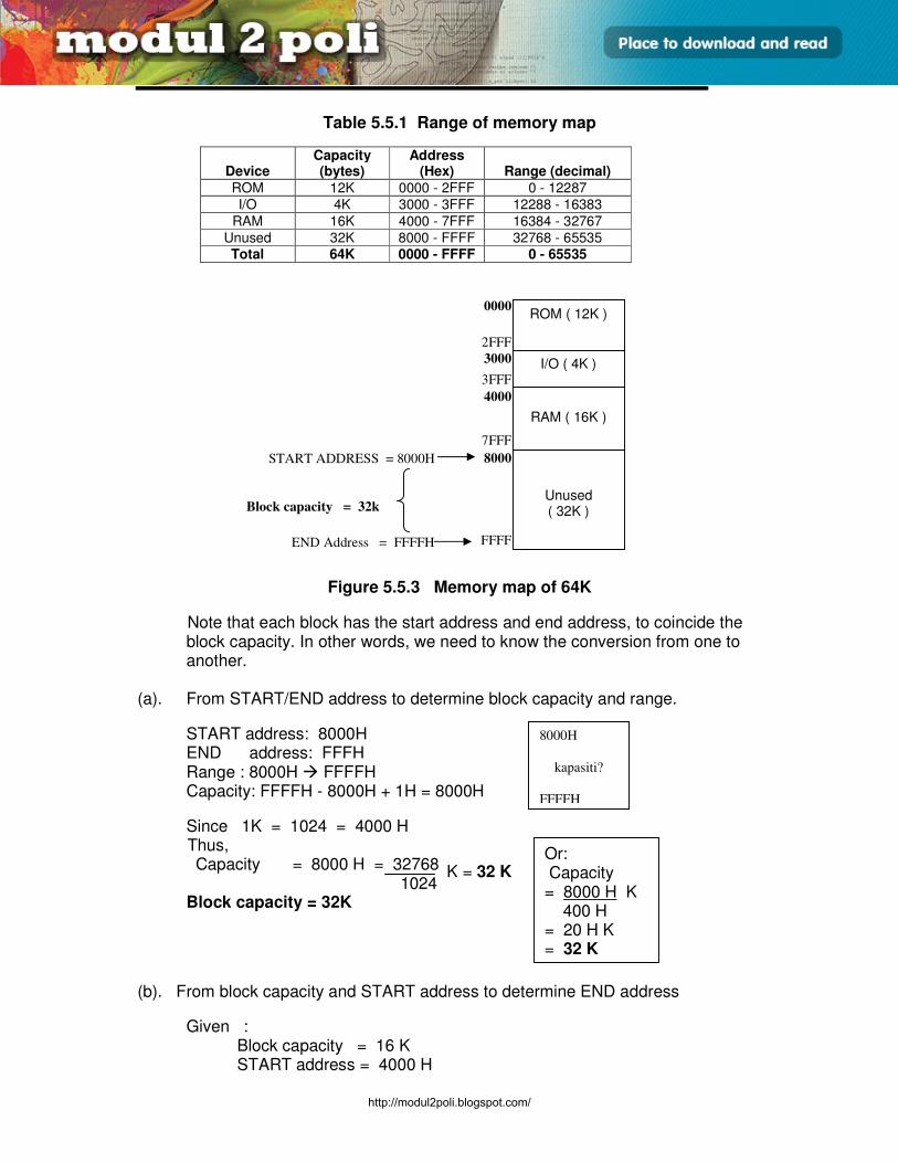
E3165 / UNIT 5 / 29
SISTEM INGATAN
Table 5.5.1 Range of memory map
Figure 5.5.3 Memory map of 64K
Note that each block has the start address and end address, to coincide the block capacity. In other words, we need to know the conversion from one to another.
(a). From START/END address to determine block capacity and range.
START address: 8000H END address: FFFH Range : 8000H FFFFH Capacity: FFFFH - 8000H + 1H = 8000H
Since 1K = 1024 = 4000 H Thus,
Capacity = 8000 H = 32768 1024 Block capacity = 32K
(b). From block capacity and START address to determine END address
Given : Block capacity = 16 K START address = 4000 H
K = 32 K
Device Capacity (bytes)
Address (Hex) Range (decimal)
ROM 12K 0000 - 2FFF 0 - 12287
I/O 4K 3000 - 3FFF 12288 - 16383
RAM 16K 4000 - 7FFF 16384 - 32767
Unused 32K 8000 - FFFF 32768 - 65535 Total 64K 0000 - FFFF 0 - 65535
START ADDRESS = 8000H
Block capacity = 32k
END Address = FFFFH
0000
2FFF
3000
3FFF
4000
7FFF
8000
FFFF
Unused ( 32K )
ROM ( 12K )
RAM ( 16K )
I/O ( 4K )
Or: Capacity = 8000 H K 400 H = 20 H K = 32 K
8000H
kapasiti?
FFFFH
http://modul2poli.blogspot.com/
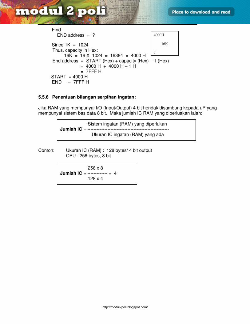
E3165 / UNIT 5 / 30
SISTEM INGATAN
Find END address = ?
Since 1K = 1024 Thus, capacity in Hex: 16K = 16 X 1024 = 16384 = 4000 H End address = START (Hex) + capacity (Hex) – 1 (Hex) = 4000 H + 4000 H – 1 H = 7FFF H START = 4000 H END = 7FFF H
5.5.6 Penentuan bilangan serpihan ingatan: Jika RAM yang mempunyai I/O (Input/Output) 4 bit hendak disambung kepada uP yang mempunyai sistem bas data 8 bit. Maka jumlah IC RAM yang diperluakan ialah: Contoh: Ukuran IC (RAM) : 128 bytes/ 4 bit output CPU : 256 bytes, 8 bit
Sistem ingatan (RAM) yang diperlukan Jumlah IC = ----------------------------------------------------- Ukuran IC ingatan (RAM) yang ada
256 x 8 Jumlah IC = ------------- = 4 128 x 4
4000H
16K
?
http://modul2poli.blogspot.com/
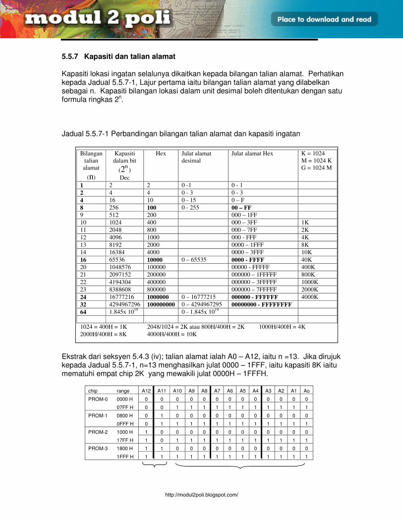
E3165 / UNIT 5 / 31
SISTEM INGATAN
5.5.7 Kapasiti dan talian alamat Kapasiti lokasi ingatan selalunya dikaitkan kepada bilangan talian alamat. Perhatikan kepada Jadual 5.5.7-1, Lajur pertama iaitu bilangan talian alamat yang dilabelkan sebagai n. Kapasiti bilangan lokasi dalam unit desimal boleh ditentukan dengan satu formula ringkas 2n. Jadual 5.5.7-1 Perbandingan bilangan talian alamat dan kapasiti ingatan Ekstrak dari seksyen 5.4.3 (iv); talian alamat ialah A0 – A12, iaitu n =13. Jika dirujuk kepada Jadual 5.5.7-1, n=13 menghasilkan julat 0000 – 1FFF, iaitu kapasiti 8K iaitu mematuhi empat chip 2K yang mewakili julat 0000H – 1FFFH.
Bilangan
talian
alamat
(n)
Kapasiti
dalam bit
(2n
)
Dec
Hex Julat alamat
desimal
Julat alamat Hex K = 1024
M = 1024 K
G = 1024 M
1 2 2 0 -1 0 - 1
2 4 4 0 - 3 0 - 3
4 16 10 0 - 15 0 – F
8 256 100 0 - 255 00 – FF
9 512 200 000 – 1FF
10 1024 400 000 – 3FF 1K
11 2048 800 000 – 7FF 2K
12 4096 1000 000 - FFF 4K
13 8192 2000 0000 – 1FFF 8K
14 16384 4000 0000 – 3FFF 10K
16 65536 10000 0 – 65535 0000 - FFFF 40K
20 1048576 100000 00000 - FFFFF 400K
21 2097152 200000 000000 – 1FFFFF 800K
22 4194304 400000 000000 – 3FFFFF 1000K
23 8388608 800000 000000 – 7FFFFF 2000K
24 16777216 1000000 0 – 16777215 000000 - FFFFFF 4000K
32 4294967296 100000000 0 – 4294967295 00000000 - FFFFFFFF
64 1.845x 10¹⁹
0 - 1.845x 10¹⁹
1024 = 400H = 1K 2048/1024 = 2K atau 800H/400H = 2K 1000H/400H = 4K
2000H/400H = 8K 4000H/400H = 10K
chip range A12 A11 A10 A9 A8 A7 A6 A5 A4 A3 A2 A1 Ao
PROM-0 0000 H 0 0 0 0 0 0 0 0 0 0 0 0 0
07FF H 0 0 1 1 1 1 1 1 1 1 1 1 1
PROM-1 0800 H 0 1 0 0 0 0 0 0 0 0 0 0 0
0FFF H 0 1 1 1 1 1 1 1 1 1 1 1 1
PROM-2 1000 H 1 0 0 0 0 0 0 0 0 0 0 0 0
17FF H 1 0 1 1 1 1 1 1 1 1 1 1 1
PROM-3 1800 H 1 1 0 0 0 0 0 0 0 0 0 0 0
1FFF H 1 1 1 1 1 1 1 1 1 1 1 1 1
http://modul2poli.blogspot.com/
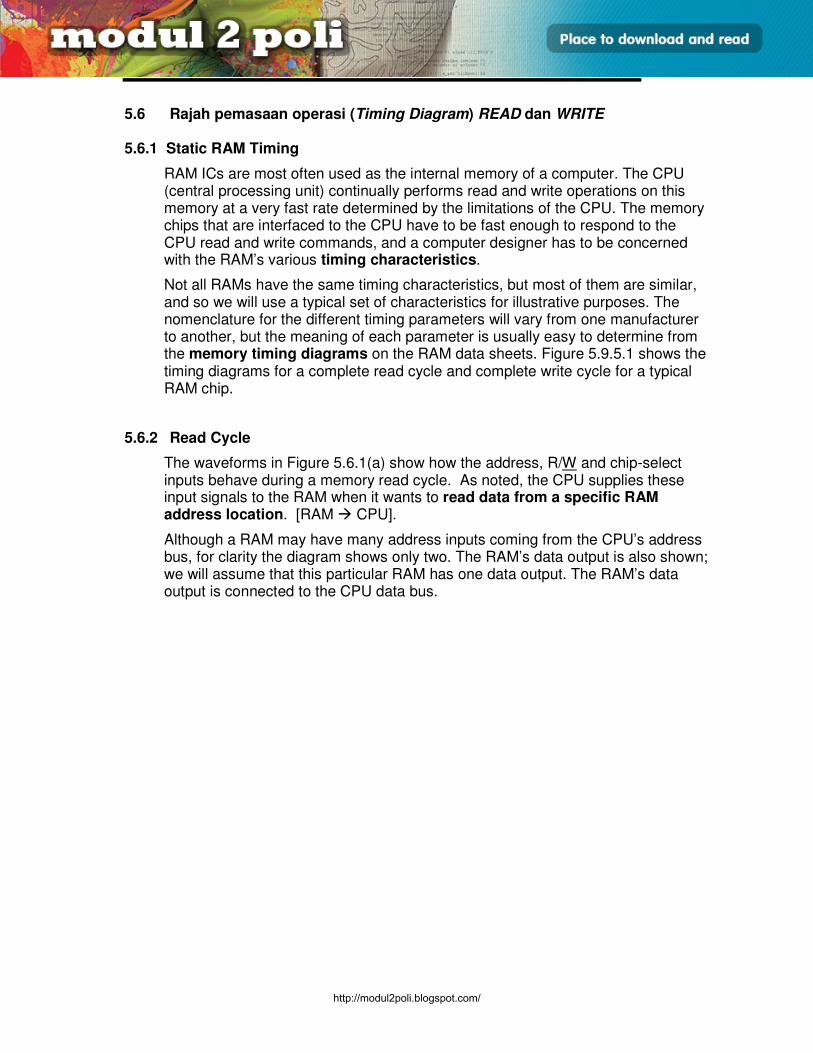
E3165 / UNIT 5 / 32
SISTEM INGATAN
5.6 Rajah pemasaan operasi (Timing Diagram) READ dan WRITE 5.6.1 Static RAM Timing
RAM ICs are most often used as the internal memory of a computer. The CPU (central processing unit) continually performs read and write operations on this memory at a very fast rate determined by the limitations of the CPU. The memory chips that are interfaced to the CPU have to be fast enough to respond to the CPU read and write commands, and a computer designer has to be concerned with the RAM’s various timing characteristics.
Not all RAMs have the same timing characteristics, but most of them are similar, and so we will use a typical set of characteristics for illustrative purposes. The nomenclature for the different timing parameters will vary from one manufacturer to another, but the meaning of each parameter is usually easy to determine from the memory timing diagrams on the RAM data sheets. Figure 5.9.5.1 shows the timing diagrams for a complete read cycle and complete write cycle for a typical RAM chip.
5.6.2 Read Cycle
The waveforms in Figure 5.6.1(a) show how the address, R/W and chip-select inputs behave during a memory read cycle. As noted, the CPU supplies these input signals to the RAM when it wants to read data from a specific RAM address location. [RAM CPU].
Although a RAM may have many address inputs coming from the CPU’s address bus, for clarity the diagram shows only two. The RAM’s data output is also shown; we will assume that this particular RAM has one data output. The RAM’s data output is connected to the CPU data bus.
http://modul2poli.blogspot.com/
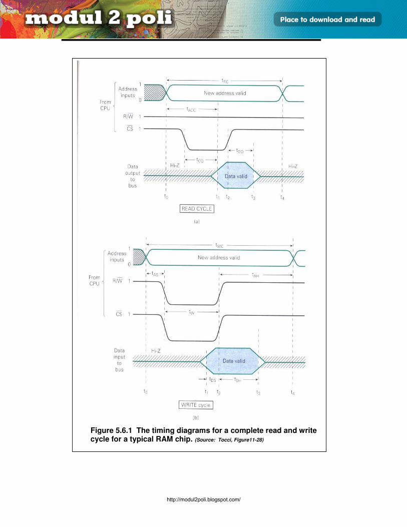
E3165 / UNIT 5 / 33
SISTEM INGATAN
Figure 5.6.1 The timing diagrams for a complete read and write cycle for a typical RAM chip. (Source: Tocci, Figure11-28)
http://modul2poli.blogspot.com/
E3165 / UNIT 5 / 34
SISTEM INGATAN
Before t0: [Address input: Old address ; R/W =1 (Read) ; CS =1 =Disable; data = Hi-Z]
The read cycle begins at time t0. Prior to that time, the address inputs will be whatever address is on the address bus from the preceding operation. Since the RAM’s chip-select is not active, it will not respond to this “old” address. Note that the R/W line is HIGH prior to t0 and stays HIGH throughout the read cycle. In most memory systems, R/W is normally kept in the HIGH state except when it is driven LOW during a write cycle. The RAM’s data output is in its Hi-Z state since CS = 1.
At t0: [Address input: Old New ; R/W =1 (Read) ; CS =1 =Disable ; Data = Hi-Z]
At t0, the CPU applies a new address to the RAM inputs; this is the address of the location to be read. After allowing time for the address signals to stabilize, the CS line is activated. The time between t0 and t1 is the RAM’s access time, tAcc, and it is the time between the application of the new address and the appearance of valid output data. The timing parameter, tCO, is the time it takes for the RAM output to go from Hi-Z to a valid data level once CS is activated (NGT).
At t1: [Address input: New ON ; R/W =1 (Read) ; CS =0 = Enable ; Data ON]
The RAM responds by placing the data from the addressed location onto the data output line at t1.
At t2: [Address input: New ON ; R/W =1 (Read) ; CS = PGT =Disable ; Data = ON]
At time t2 the CS is returned HIGH, and the RAM output returns to its Hi-Z state after a time interval, tOD [t2 t3]. Thus, the RAM data will be on the data bus between t1 and t3. The CPU can take it from the data bus at any point during this interval. In most computers, the CPU will use the PGT of the CS signal at t2 to latch these data into one of its internal registers.
At t3: [Address input: New ON ; R/W =1 (Read) ; CS =1 =Disable ; Data = OFF]
At t3, the data is removed from the data bus (go back to Hi-Z).
At t4: [Address input: Start of next address; R/W =1 (Read); CS =1 =Disable; Data =Hi-Z]
The complete read cycle time, tRC, extends from t0 to t4, At t4, the CPU changes the address inputs to a different address for the next read or Read/Write cycle.
http://modul2poli.blogspot.com/
E3165 / UNIT 5 / 35
SISTEM INGATAN
5.6.3 Write Cycle
Figure 5.22(b) shows the signal activity for a write cycle that begins when the CPU supplies a new address to the RAM at a time t0,.
At t0: [Address input: Old New ; R/W =1 (Write Disable); CS =1 =Disable; Data = Hi-Z]
At t0, the CPU applies a new address to the RAM inputs; this is the address of the location to be written.
tAS: [Address input: Old New ; R/W =NGT (Write) ; CS =NGT = Enable ; Data = Hi-Z]
The CPU drives the R/W and CS lines LOW after waiting for a time interval tAS, called the address setup time. This give the RAM’s address decoder time to respond to the new address.
tW: [Address input: Old New ; R/W =NGT↔ PGT ( Write) ; CS =NGT ↔ PGT =Enable ; Data = ON]
R/W and CS are held LOW for a time interval tW, called the write time interval.
At t1: [Address input: Stay ; R/W =0 (Write) ; CS =0 =Enable ; Data = Hi-Z ON]
During this write-time interval; at time t1, the CPU applies valid data to the data bus to be written into the RAM.
At t2: [Address input: Stay ; R/W =PGT (Reset Write) ; CS =PGT =Disable ; Data = ON]
These data have to be held at the RAM input for at least a time interval tDS prior to, and for at least a time interval tDH after, the deactivation of R/W and CS at t2. The tDS interval is called the data setup time, and tDH is called the data hold time.
At t3: [Address input: Stay ; R/W =1 (Write Disable) ; CS =1 = Disable ; Data = Hi-Z]
At t3, the data is removed from the data bus (go back to Hi-Z).
Similarly, the address inputs have to remain stable for the address hold-time interval, tAH, after t2. If any of these setup- or hold-time requirements are not met, the write operation will not take place reliably.
At t4: [Address input: Start of next address; R/W =1 (Write Disable); CS =1 =Disable; Data =Hi-Z]
The complete read cycle time, tWC, extends from t0 to t4, At t4, the CPU changes the address inputs to a different address for the next read or write cycle.
The read cycle time, tRC, and write cycle time, twc , are what essentially determine how fast a memory chip can operate. For example, in an actual application, a CPU will often be reacting successive data words from memory one right after the other. If the memory has a tRC of 50 ns, the CPU can read one word every 50 ns, or 20 million words per second; with tRC = 10 ns, the CPU can read 100 million words per second. Table
http://modul2poli.blogspot.com/
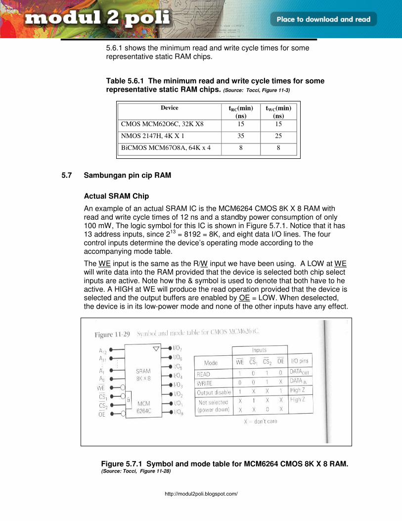
E3165 / UNIT 5 / 36
SISTEM INGATAN
5.6.1 shows the minimum read and write cycle times for some representative static RAM chips.
Table 5.6.1 The minimum read and write cycle times for some representative static RAM chips. (Source: Tocci, Figure 11-3)
5.7 Sambungan pin cip RAM
Actual SRAM Chip
An example of an actual SRAM IC is the MCM6264 CMOS 8K X 8 RAM with read and write cycle times of 12 ns and a standby power consumption of only 100 mW, The logic symbol for this IC is shown in Figure 5.7.1. Notice that it has 13 address inputs, since 213 = 8192 = 8K, and eight data I/O lines. The four control inputs determine the device’s operating mode according to the accompanying mode table.
The WE input is the same as the R/W input we have been using. A LOW at WE will write data into the RAM provided that the device is selected both chip select inputs are active. Note how the & symbol is used to denote that both have to he active. A HIGH at WE will produce the read operation provided that the device is selected and the output buffers are enabled by OE = LOW. When deselected, the device is in its low-power mode and none of the other inputs have any effect.
Figure 5.7.1 Symbol and mode table for MCM6264 CMOS 8K X 8 RAM. (Source: Tocci, Figure 11-28)
Device tRC(min)
(ns)
tWC(min)
(ns)
CMOS MCM62O6C, 32K X8 15 15
NMOS 2147H, 4K X 1 35 25
BiCMOS MCM67O8A, 64K x 4 8 8
http://modul2poli.blogspot.com/
E3165 / UNIT / 1
INPUT/OUTPUT AND INTERFACE
Objektif Am:
Mengetahui dan memahami masukan/keluaran (I/O) dan perantaramuka
Obektif Khusus:
UNIT 6
OBJECTIVE
MASUKAN/KELUARAN DAN PERANTARAMUKA 15. Operasi input/output:
Menerangkan pemindahan terus. Menerangkan sampukan Menerangkan ingatan Capaian Terus (DMA) Menerangkan jabat-tangan (hand-shaking)
16. Teknik-teknik memasukkan dan mengeluarkan data dari komputer bersiri atau selari. Menerangkan teknik-teknik penghantaran data siri dan selari Menerangkan ciri-ciri perantaramuka selari dan siri. Menerangkan ciri komunikasi bersiri tak segerak; bit mula, bit henti, bit pariti dan
kadar baud. Menerangkan komunikasi bersiri segerak, kawalan rangkaian data bersiri, akasara
segerak. 17. PPI 8255A/PIA 6821
Menerangkan gambarajah blok dan fungsi daftar dalaman PPI8255A/PIA6821 Menerangkan proses pengaturacaraan antaramuka input/output PPI
8255A/PIA6821
18. Menerangkan fungsi dan contoh litar antaramuka input/output seperti; ADC/DAC Litar pemacu kawalan motor Litar kawalan masukan/keluaran.
http://modul2poli.blogspot.com/
E3165 / UNIT / 2
INPUT/OUTPUT AND INTERFACE
MASUKAN/KELUARAN DAN PERANTARAMUKA 15. Operasi input/output:
Peranti Masukan dan Keluaran (I/O): Ialah satu medium untuk membolehkan komputer mendapatkan maklumat dari luar untuk
diproses dalam komputer dan hasilnya dikeluarkan semula ke luar sistem komputer.
Dengan kata lain, peranti I/O juga merupakan suatu perantaramuka.
Lima (5) sebab mengapa perantaramuka diperlukan:
i. Sebagai storan sementara untuk data yang dipindahkan di antara komputer
dan peranti luar.
ii. Memberi isyarat kepada komputer jika terdapat ralat semasa data
dipindahkan.
iii. Memberi isyarat kepada komputer sekiranya operasi perpindahan data
selesai.
iv. Kadar perpindahan data dari alat persisian mesti disegerakkan dengan
kendalian CPU dan ingatan.
v. Kadar perpindahan data di antara perlatan luar dan sistem mikro komputer
berlainan. Kaedah Pemindahan data Tga cara asas yang digunakan untuk pemindahan data dari sesuatu peranti peripheral: i. Polling (Tinjauan) ii. Interrupt (Sampukan) iii. DMA (Direct Memory Access)
Menerangkan pemindahan terus.
Kaedah pemindahan terus lebih dikenali sebagai Polling. Daedah ini di mana
mikropemproses memeriksa keadaan peranti I/O terlebih dahulu samada is bersedia
menerima arahan daripada mikropemproses.
Menerangkan sampukan.
Sampukan (Interrupt):
Interrupt (sampukan) ialah isyarat yang akan menyebabkan mikropemproses berhenti
melaksanakan operasi/jujukan biasa
Tafsiran Sampukan yang lain ialah: Isyarat luar yang menggantung sementara aturcara
yang sedang dilaksanakan oleh mikropemproses, dan menyebabkan kawalan aturcara
dipindah ke sub rutin yang direka untuk memberi khidmat kepada sampukan tersebut.
INPUT-6A
http://modul2poli.blogspot.com/
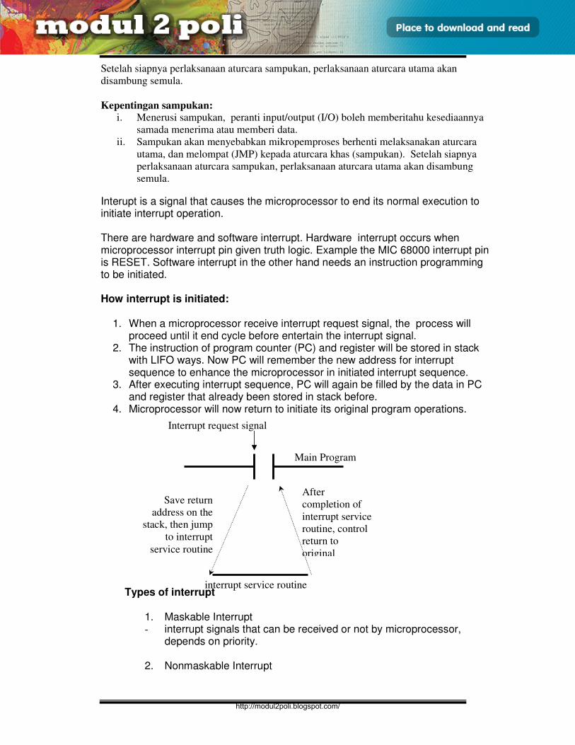
E3165 / UNIT / 3
INPUT/OUTPUT AND INTERFACE
Setelah siapnya perlaksanaan aturcara sampukan, perlaksanaan aturcara utama akan
disambung semula.
Kepentingan sampukan:
i. Menerusi sampukan, peranti input/output (I/O) boleh memberitahu kesediaannya
samada menerima atau memberi data.
ii. Sampukan akan menyebabkan mikropemproses berhenti melaksanakan aturcara
utama, dan melompat (JMP) kepada aturcara khas (sampukan). Setelah siapnya
perlaksanaan aturcara sampukan, perlaksanaan aturcara utama akan disambung
semula.
Interupt is a signal that causes the microprocessor to end its normal execution to initiate interrupt operation. There are hardware and software interrupt. Hardware interrupt occurs when microprocessor interrupt pin given truth logic. Example the MIC 68000 interrupt pin is RESET. Software interrupt in the other hand needs an instruction programming to be initiated. How interrupt is initiated:
1. When a microprocessor receive interrupt request signal, the process will
proceed until it end cycle before entertain the interrupt signal. 2. The instruction of program counter (PC) and register will be stored in stack
with LIFO ways. Now PC will remember the new address for interrupt sequence to enhance the microprocessor in initiated interrupt sequence.
3. After executing interrupt sequence, PC will again be filled by the data in PC and register that already been stored in stack before.
4. Microprocessor will now return to initiate its original program operations.
Types of interrupt
1. Maskable Interrupt - interrupt signals that can be received or not by microprocessor,
depends on priority. 2. Nonmaskable Interrupt
After
completion of
interrupt service
routine, control
return to
original
Interrupt request signal
Main Program
Save return
address on the
stack, then jump
to interrupt
service routine
interrupt service routine
http://modul2poli.blogspot.com/

E3165 / UNIT / 4
INPUT/OUTPUT AND INTERFACE
- interrupt signal that must be received by the microprocessor.
The interrupt advantage
1. To ensure the I/O devices or peripheral devices interrupting
microprocessor to initiate. 2. Reduce time and cost in such away that interrupt only occurs when
microprocessor receive an interrupt signal.
http://modul2poli.blogspot.com/

E3165 / UNIT / 5
INPUT/OUTPUT AND INTERFACE
Menerangkan ingatan Capaian Terus (DMA)
Ingatan Capaian Terus (Direct Memory Access/ DMA):
DMA ialah peranti memori perantaraan yang boleh dicapai terus antara I/O dan Memory
tanpa melalui CPU.
Data dipindahkan antara ingatan dan komponen lain yang dikawal secara luaran. Ini
bermakna mikropemproses tidak terlibat dalam proses pemindahan ini.
Ia digunakan untuk mengurangkan masa yang diambil untuk pemindahan data di antara
peranti I/O dan mikropemproses.
http://modul2poli.blogspot.com/
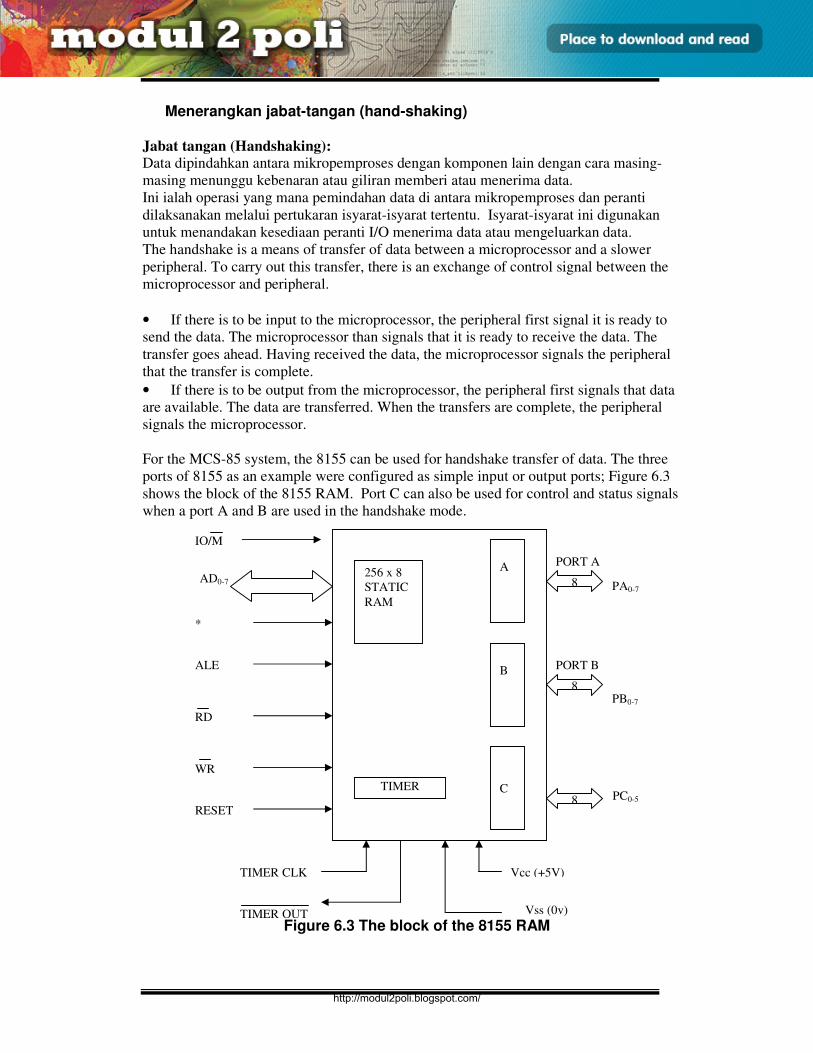
E3165 / UNIT / 6
INPUT/OUTPUT AND INTERFACE
Menerangkan jabat-tangan (hand-shaking)
Jabat tangan (Handshaking):
Data dipindahkan antara mikropemproses dengan komponen lain dengan cara masing-
masing menunggu kebenaran atau giliran memberi atau menerima data.
Ini ialah operasi yang mana pemindahan data di antara mikropemproses dan peranti
dilaksanakan melalui pertukaran isyarat-isyarat tertentu. Isyarat-isyarat ini digunakan
untuk menandakan kesediaan peranti I/O menerima data atau mengeluarkan data.
The handshake is a means of transfer of data between a microprocessor and a slower
peripheral. To carry out this transfer, there is an exchange of control signal between the
microprocessor and peripheral.
• If there is to be input to the microprocessor, the peripheral first signal it is ready to
send the data. The microprocessor than signals that it is ready to receive the data. The
transfer goes ahead. Having received the data, the microprocessor signals the peripheral
that the transfer is complete.
• If there is to be output from the microprocessor, the peripheral first signals that data
are available. The data are transferred. When the transfers are complete, the peripheral
signals the microprocessor.
For the MCS-85 system, the 8155 can be used for handshake transfer of data. The three
ports of 8155 as an example were configured as simple input or output ports; Figure 6.3
shows the block of the 8155 RAM. Port C can also be used for control and status signals
when a port A and B are used in the handshake mode.
Figure 6.3 The block of the 8155 RAM
PA0-7
PB0-7
256 x 8
STATIC
RAM
TIMER
A
B
C
PORT A
8
PORT B
8
8 PC0-5
TIMER CLK
TIMER OUT
IO/M
Vcc (+5V)
Vss (0v)
AD0-7
*
ALE
RD
WR
RESET
http://modul2poli.blogspot.com/

E3165 / UNIT / 7
INPUT/OUTPUT AND INTERFACE
16. Teknik-teknik memasukkan dan mengeluarkan data dari komputer
bersiri atau selari.
Pengantaramukaan: Suatu kaedah yang digunakan untuk menggandingkan peranti luar dengan sistem komputer
dan juga mengubah bentuk kuantiti di luar komputer supaya dapat disesuaikan dengan
sistem komputer, atau sebaliknya mengubah kembali data dari sistem komputer untuk
disesuaikan dengan peranti luar.
Adakalanya I/O juga dirujuk sebagai perantara muka atau sebaliknya.
Menerangkan teknik-teknik penghantaran data siri dan selari.
Teknik Penghantaran data:
Penghantaran data ialah satu proses memindahkan data dari satu titik ke titik yang lain,
dengan kata lain, dari suatu sumber ke suatu destinasi. Kedua-dua hujung ini biasanya
dihubungkan dengan satu media penghantaran. Corak penghantaran yang berlaku pada
media penghantaran ialah teknik penghantaran. Terdapat dua teknik iaitu siri dan selari.
Penghantaran data secara selari: Data dihantar lebih daripada satu bit secara serentak dalam satu-satu masa. Contohnya
pemindahan/penghantaran data di antara mikropemproses dan peranti-peranti 8-bit yang
lain secara serentak.
Memudahkan rekabentuk sistem kerana ia boleh diaturcara untuk fungsi input, output atau
kedua-dua sekali.
Digunakan untuk banyak aplikasi dengan hanya menambah litar yang sesuai.
Ia mempunyai isyarat ‘handshaking’ yang memudahkan antaramuka dengan peranti seperti
litar penukar ADC, DAC dan pencetak selari.
Berkeupayaan mengendalikan sampukan.
Penghantaran data secara siri: Data dihantar hanya satu bit sahaja dalam satu-satu masa. Blok data akan dihantar satu per
satu melalui talian yang sama. Contohnya pemindahan/penghantaran data di antara papan
kekunci dan peranti antaramuka siri 1-bit sahaja).
http://modul2poli.blogspot.com/
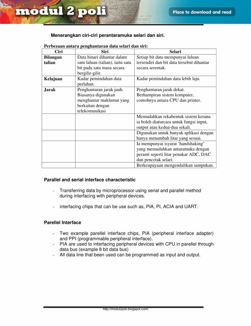
E3165 / UNIT / 8
INPUT/OUTPUT AND INTERFACE
Menerangkan ciri-ciri perantaramuka selari dan siri.
Perbezaan antara penghantaran data selari dan siri:
Ciri Siri Selari
Bilangan
talian
Data binari dihantar dalam
satu laluan (talian), iaitu satu
bit pada satu masa secara
bergilir-gilir.
Setiap bit data mempunyai laluan
tersendiri dan bit data tersebut dihantar
secara serentak.
Kelajuan Kadar pemindahan data
perlahan.
Kadar pemindahan data lebih laju.
Jarak Penghantaran jarak jauh.
Biasanya digunakan
menghantar maklumat yang
berkaitan dengan
telekomunikasi
Penghantaran jarak dekat.
Berhampiran sistem komputer,
contohnya antara CPU dan printer.
Memudahkan rekabentuk sistem kerana
ia boleh diaturcara untuk fungsi input,
output atau kedua-dua sekali.
Digunakan untuk banyak aplikasi dengan
hanya menambah litar yang sesuai.
Ia mempunyai isyarat ‘handshaking’
yang memudahkan antaramuka dengan
peranti seperti litar penukar ADC, DAC
dan pencetak selari.
Berkeupayaan mengendalikan sampukan.
Parallel and serial interface characteristic
- Transferring data by microprocessor using serial and parallel method during interfacing with peripheral devices.
- interfacing chips that can be use such as, PIA, PI, ACIA and UART.
Parellel Interface
- Two example parellel interface chips, PIA (peripheral interface adapter) and PPI (programmable peripheral interface).
- PIA are used to interfacing peripheral devices with CPU in parellel through data bus (example 8 bit data bus)
- All data line that been used can be programmed as input and output.
http://modul2poli.blogspot.com/
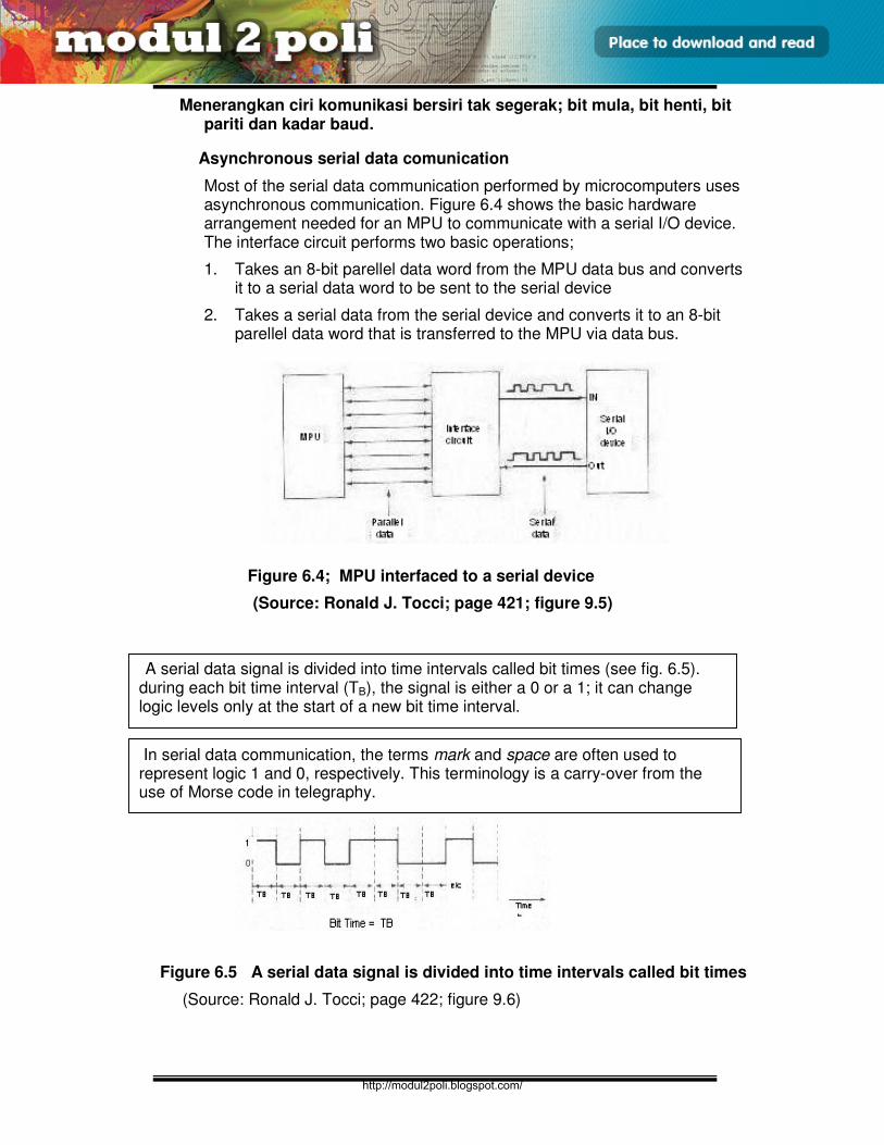
E3165 / UNIT / 9
INPUT/OUTPUT AND INTERFACE
Menerangkan ciri komunikasi bersiri tak segerak; bit mula, bit henti, bit pariti dan kadar baud.
Asynchronous serial data comunication
Most of the serial data communication performed by microcomputers uses asynchronous communication. Figure 6.4 shows the basic hardware arrangement needed for an MPU to communicate with a serial I/O device. The interface circuit performs two basic operations;
1. Takes an 8-bit parellel data word from the MPU data bus and converts it to a serial data word to be sent to the serial device
2. Takes a serial data from the serial device and converts it to an 8-bit parellel data word that is transferred to the MPU via data bus.
Figure 6.4; MPU interfaced to a serial device
(Source: Ronald J. Tocci; page 421; figure 9.5)
Figure 6.5 A serial data signal is divided into time intervals called bit times
(Source: Ronald J. Tocci; page 422; figure 9.6)
A serial data signal is divided into time intervals called bit times (see fig. 6.5). during each bit time interval (TB), the signal is either a 0 or a 1; it can change logic levels only at the start of a new bit time interval.
In serial data communication, the terms mark and space are often used to represent logic 1 and 0, respectively. This terminology is a carry-over from the use of Morse code in telegraphy.
http://modul2poli.blogspot.com/
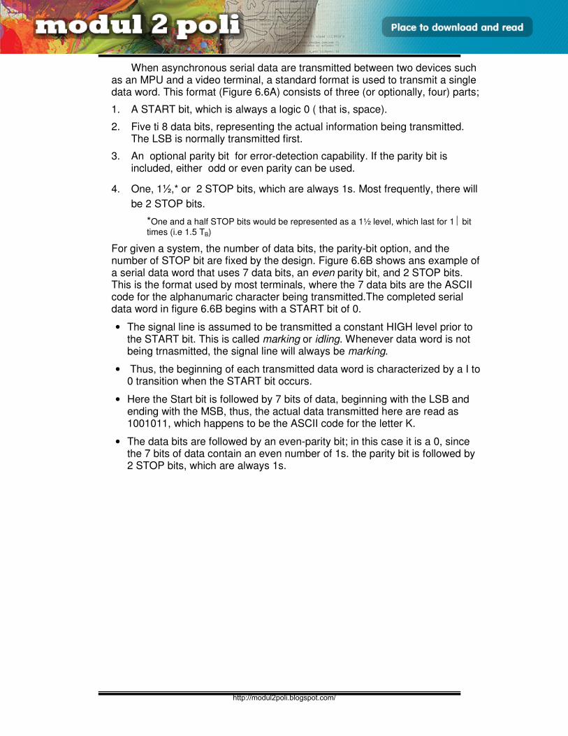
E3165 / UNIT / 10
INPUT/OUTPUT AND INTERFACE
When asynchronous serial data are transmitted between two devices such as an MPU and a video terminal, a standard format is used to transmit a single data word. This format (Figure 6.6A) consists of three (or optionally, four) parts;
1. A START bit, which is always a logic 0 ( that is, space).
2. Five ti 8 data bits, representing the actual information being transmitted. The LSB is normally transmitted first.
3. An optional parity bit for error-detection capability. If the parity bit is included, either odd or even parity can be used.
4. One, 1½,* or 2 STOP bits, which are always 1s. Most frequently, there will
be 2 STOP bits.
*One and a half STOP bits would be represented as a 1½ level, which last for 1 bit times (i.e 1.5 TB)
For given a system, the number of data bits, the parity-bit option, and the number of STOP bit are fixed by the design. Figure 6.6B shows ans example of a serial data word that uses 7 data bits, an even parity bit, and 2 STOP bits. This is the format used by most terminals, where the 7 data bits are the ASCII code for the alphanumaric character being transmitted.The completed serial data word in figure 6.6B begins with a START bit of 0.
• The signal line is assumed to be transmitted a constant HIGH level prior to the START bit. This is called marking or idling. Whenever data word is not being trnasmitted, the signal line will always be marking.
• Thus, the beginning of each transmitted data word is characterized by a I to 0 transition when the START bit occurs.
• Here the Start bit is followed by 7 bits of data, beginning with the LSB and ending with the MSB, thus, the actual data transmitted here are read as 1001011, which happens to be the ASCII code for the letter K.
• The data bits are followed by an even-parity bit; in this case it is a 0, since the 7 bits of data contain an even number of 1s. the parity bit is followed by 2 STOP bits, which are always 1s.
http://modul2poli.blogspot.com/
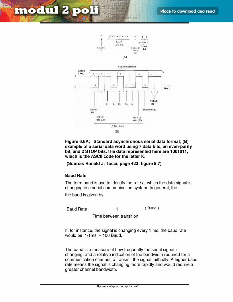
E3165 / UNIT / 11
INPUT/OUTPUT AND INTERFACE
Figure 6.6A; Standard asynchronous serial data format; (B) example of a serial data word using 7 data bits, an even-parity bit, and 2 STOP bits. tHe data represented here are 1001011, which is the ASCII code for the letter K.
(Source: Ronald J. Tocci; page 423; figure 9.7)
Baud Rate
The term baud is use to identify the rate at which the data signal is changing in a serial communication system. In general, the
the baud is given by
Baud Rate = 1
Time between transition
If, for instance, the signal is changing every 1 ms, the baud rate would be 1/1ms = 100 Baud.
The baud is a measure of how frequently the serial signal is changing, and a relative indication of the bandwidth required for a communication channel to transmit the signal faithfully. A higher baud rate means the signal is changing more rapidly and would require a greater channel bandwidth.
( Baud )
http://modul2poli.blogspot.com/
E3165 / UNIT / 12
INPUT/OUTPUT AND INTERFACE
In some situation, but not always, the baud rate is equivalent to the rate at which data bits are being transferred. For example, in the standard asynchronous serial data format (figure 6.6 ) a new bit is sent every bit time interval (TB), so that data bits are being transferred at rate given by
Data Rate = 1
TB
If TB = 1 ms, the data rate becomes 1000 bits/s. the baud rate ia also 1000 because the time between signal transition is equal to 1 ms. Thus, in this simple serial data format the baud rate and data rate are the same, although they are expressed in different units – 1000 bits/s versus 1000 Baud.
Example xxx – pg 425
A certain video display terminal is operating at a baud rate of 9600 using the standard asynchronous serial format. What is the time duration of one bit in the serial data going to and from from this terminal?
Solution;
For this situation the baud rate and data rate are the same. Thus, since data rate = 9600 bits/s, the bit time will be 1/9600 = 104.17
µs.
(bita/s)
http://modul2poli.blogspot.com/
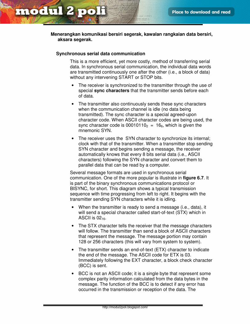
E3165 / UNIT / 13
INPUT/OUTPUT AND INTERFACE
Menerangkan komunikasi bersiri segerak, kawalan rangkaian data bersiri, aksara segerak.
Synchronous serial data communication
This is a more efficient, yet more costly, method of transferring serial data. In synchronous serial communication, the individual data words are transmitted continuously one after the other (i.e., a block of data) without any intervening START or STOP bits.
• The receiver is synchronized to the transmitter through the use of special sync characters that the transmitter sends before each of data.
• The transmitter also continuously sends these sync characters when the communication channel is idle (no data being transmitted). The sync character is a special agreed-upon character code. When ASCII character codes are being used, the sync character code is 000101102 = 166, which is given the mnemonic SYN.
• The receiver uses the SYN character to synchronize its internal; clock with that of the transmitter. When a transmitter stop sending SYN character and begins sending a message, the receiver automatically knows that every 8 bits serial data (i.e., ASCII characters) following the SYN character and convert them to parallel data that can be read by a computer.
Several message formats are used in synchronous serial communication. One of the more popular is illustrate in figure 6.7. It is part of the binary synchronous communications protocol or BISYNC, for short. This diagram shows a typical transmission sequence with time progressing from left to right. It begins with the transmitter sending SYN characters while it is idling.
• When the transmitter is ready to send a message (i.e., data), it will send a special character called start-of-text (STX) which in ASCII is 0216.
• The STX character tells the receiver that the message characters will follow. The transmitter than send a block of ASCII characters that represent the message. The message portion may contain 128 or 256 characters (this will vary from system to system).
• The transmitter sends an end-of-text (ETX) character to indicate the end of the message. The ASCII code for ETX is 03. Immediately following the EXT character, a block check character (BCC) is sent.
• BCC is not an ASCII code; it is a single byte that represent some complex parity information calculated from the data bytes in the message. The function of the BCC is to detect if any error has occurred in the transmission or reception of the data. The
http://modul2poli.blogspot.com/
E3165 / UNIT / 14
INPUT/OUTPUT AND INTERFACE
receiver can recalculate its own BCC from the data in the message, and compare it with the BCC sent by the transmitter. If they are different, the receiver can send a message to the transmitter requesting that it send its previous message over again.
• After the BCC character, the transmitter can send the next portion of the message by first sending two SYN characters which the receiver can use to resynchronize its clock, followed by an STX character and the data. If the transmitter has no more data to send (i.e. the complete message has been sent), it will send continuous SYN characters.
Synchronous communication is more efficient than asynchronous because only about 2 or 3 percent of the transmitted data is taken up by SYN characters and other special characters, compared to about 20 percent for asynchronous. However the transmitter and receiver circuitry for synchronous operation is more complex.
Figure 6.7; Typical transmission synchronous communication sequence using BISYNC format
(Source: Ronald J. Tocci; page 451; figure 9.17)
http://modul2poli.blogspot.com/
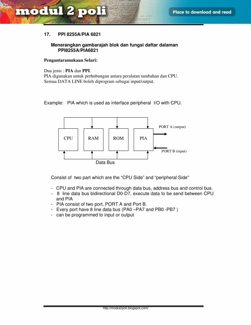
E3165 / UNIT / 15
INPUT/OUTPUT AND INTERFACE
17. PPI 8255A/PIA 6821
Menerangkan gambarajah blok dan fungsi daftar dalaman PPI8255A/PIA6821
Pengantaramukaan Selari:
Dua jenis : PIA dan PPI.
PIA digunakan untuk perhubungan antara peralatan tambahan dan CPU.
Semua DATA LINE boleh diprogram sebagai input/output.
Example: PIA which is used as interface peripheral I/O with CPU.
Consist of two part which are the “CPU Side” and “peripheral Side" - CPU and PIA are connected through data bus, address bus and control bus. - 8 line data bus bidirectional D0-D7, execute data to be send between CPU
and PIA - PIA consist of two port, PORT A and Port B. - Every port have 8 line data bus (PA0 –PA7 and PB0 -PB7 ) - can be programmed to input or output
CPU
RAM
ROM
PIA
PORT A (output)
PORT B (input)
Data Bus
http://modul2poli.blogspot.com/

E3165 / UNIT / 16
INPUT/OUTPUT AND INTERFACE
Menerangkan proses pengaturacaraan antaramuka input/output PPI 8255A/PIA6821
http://modul2poli.blogspot.com/
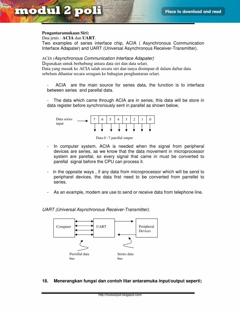
E3165 / UNIT / 17
INPUT/OUTPUT AND INTERFACE
Pengantaramukaan Siri: Dua jenis : ACIA dan UART.
Two examples of series interface chip, ACIA ( Asynchronous Communication Interface Adapater) and UART (Universal Asynchronous Receiver-Transmitter).
ACIA (Asynchronous Communication Interface Adapater) Digunakan untuk berhubung antara data siri dan data selari.
Data yang masuk ke ACIA ialah secara siri dan ianya disimpan di dalam daftar data
sebelum dihantar secara seragam ke bahagian penghantaran selari.
- ACIA are the main source for series data, the function is to interface between series and parellal data. - The data which came through ACIA are in series, this data will be store in data register before synchronously sent in parallel as shown below,
- In computer system, ACIA is needed when the signal from peripheral
devices are series, as we know that the data movement in microprocessor system are parellal, so every signal that came in must be converted to parellal signal before the CPU can process it.
- in the opposite ways , if any data from microprocessor which will be send to
peripharel devices, the data first need to be converted from parrellel to series.
- As an example, modem are use to send or receive data from telephone line.
UART (Universal Asynchronous Receiver-Transmitter).
18. Menerangkan fungsi dan contoh litar antaramuka input/output seperti;
Data 0 –7 parellal output
7 6 5 4 3 2 1 0 Data series
input
Computer
UART
Peripheral
Devices
Perrellal data
bus
Series data
bus
http://modul2poli.blogspot.com/
E3165 / UNIT / 18
INPUT/OUTPUT AND INTERFACE
ADC/DAC
ADC (Analog to Digital converter)
Menukar isyarat analog ke isyarat digital.
Keluaran digital mengandungi nombor binari yang mewakili masukan analog.
Penukar isyarat elektrik analog digunakan sebagai masukan kepada ADC.
DAC (Digital to Analog converter)
Menukar isyarat digital ke isyarat analog.
Isyarat analog seperti kuantiti voltan, manakala isyarat digital dalam binari atau kod-kod.
Litar pemacu kawalan motor
Litar kawalan masukan/keluaran.
6.1 PPI 8255A/PIA 6821
http://modul2poli.blogspot.com/
E3165 / UNIT / 19
INPUT/OUTPUT AND INTERFACE
6.3.1 Description of The Block diagram, Register Function and Programmable Interface Process.
A more in-depth look at the MC 6821 is necessary to get a full grasp of the power and flexibility that this chip provides microcomputer system designers. Figure 6.8 shows the block diagram of the MC 6821.
The chip can be thought of as two completely independent 8-bit I/O ports. Ports A and B contain data direction registers (DDRA, DDRB) wich allow the programmer to specify independently each pin of both ports as either an input or an output pin.
• Putting a “0” in a data direction register bit causes the corresponding pin on the port to act as an input.
• Placing a “ 1 “ in a particular bit position of the DDR causes the corresponding pin on the port to act as an output.
The control registers ( CRA, CRB ) allow the programmer to choose certain interrupt and peripheral control capabilities. Also, the control register provides certain status information concerning interrupt activity.
The output registers (ORA,ORB) hold data that are to be sent to output devices until such devices are ready to accept it. Inputs CA1, CA2, CB1 and CB2 can be ued as status inputs for conditional I/O transfer, or for interrupt interfacing cpabilities. Under softwarecontrol CA2 and CB2 can be programmed, via the control register, to act as peripheral control outputs that can be used in various handshaking schemes.
In dealing with this chip the MPU must be able to communicate with six different registers. In Fig. 6.8 you will notice that the CHIP SELECT and control section has only two register select inputs, RS0 and RS1.
This seems to indicate that the MPU can only communicate with four registers. However, one bit in each control register is used to distinguish between addressing of the data direction register and the output register.
R/W
http://modul2poli.blogspot.com/
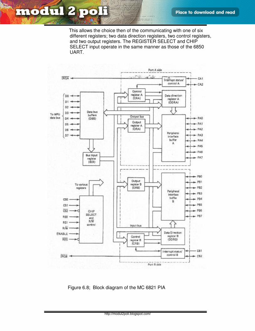
E3165 / UNIT / 20
INPUT/OUTPUT AND INTERFACE
This allows the choice then of the communicating with one of six different registers; two data direction registers, two control registers, and two output registers. The REGISTER SELECT and CHIP SELECT input operate in the same manner as those of the 6850 UART.
Figure 6.8; Block diagram of the MC 6821 PIA
http://modul2poli.blogspot.com/
E3165 / UNIT / 21
INPUT/OUTPUT AND INTERFACE
PPI 8255A
The 8255A is a programmable peripheral interface (PPI) device designed for use in Intel microcomputer systems. Its function is that of a general purposes I/O component to Interface peripheral equipment to the microcomputer system bush. The functional configuration of the 8255A is programmed by the systems software so that normally no external logic is necessary to interface peripheral devices or structures.
Data Bus Buffer
This 3-stable bi-directional 8-bit buffer is used to interface the 8255A to the systems data bus. Data is transmitted or received by the buffer upon execution of input or output instructions by the CPU. Control words and status information are also transferred through the data bus buffer. Read/Write and Control Logic
The function of this block is to manage all of the Internal and External transfers of both Data and Control or Status words. It accepts inputs from the CPU Address and Control business and in turn, issues commands to both of the Control Groups.
(CS)
Chip Select. A “low’ on this input pin enables the communication between the 8255A, and the CPU.
(RD)
Read. A “low” on this Input pin enables the 8255A to send the data or status information to the CPU on the data bus. In essence, it allows the CPU to “read from the 8255A.
(WR)
Write. A. “ low” on the input pin enables the CPU to write data or control words into the 8255A.
(A0 and A1) Port Select 0 and Port Select 1. The Input signals, in conjunction with the RD and WR Inputs, controls the selection of one of the three ports or the control word registers. They are normally connected to the least significant bits of the address bus (A0 and A1).
http://modul2poli.blogspot.com/
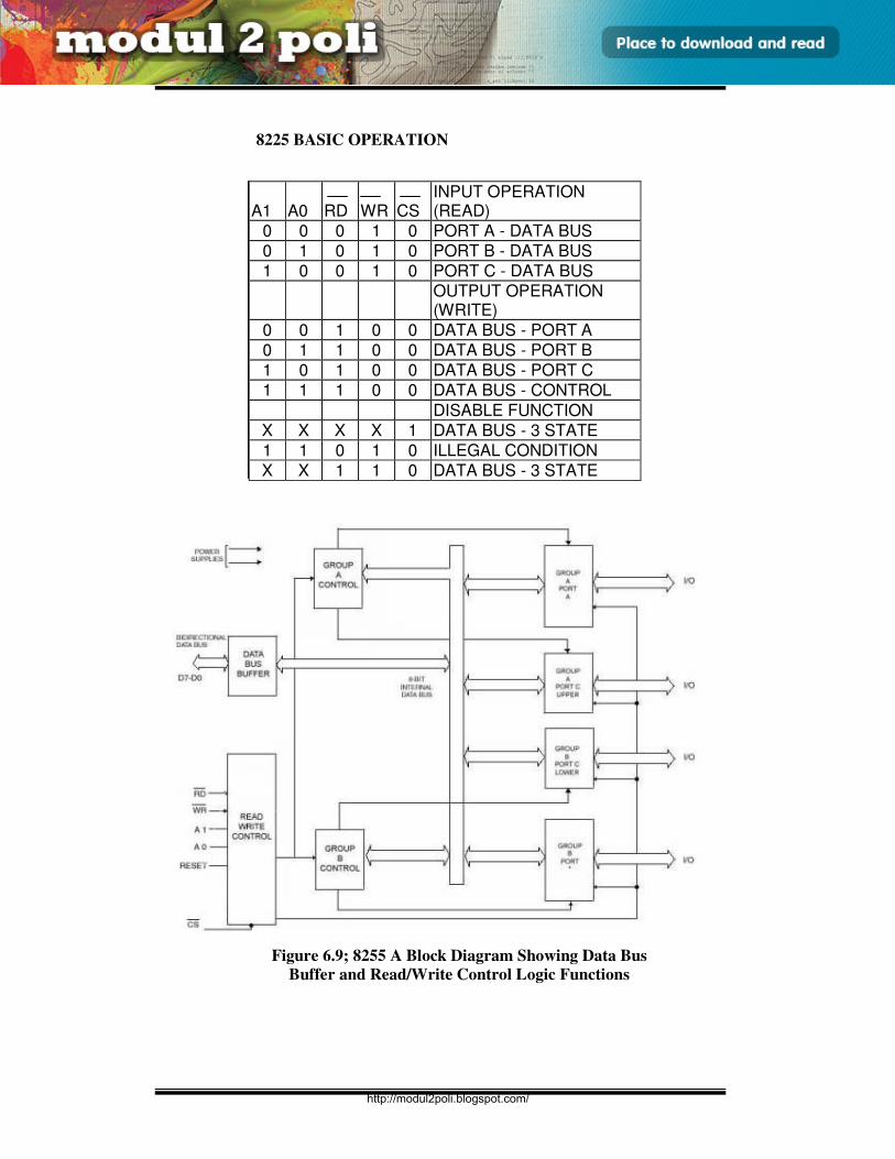
E3165 / UNIT / 22
INPUT/OUTPUT AND INTERFACE
8225 BASIC OPERATION
Figure 6.9; 8255 A Block Diagram Showing Data Bus
Buffer and Read/Write Control Logic Functions
A1
A0
RD
WR
CS
INPUT OPERATION (READ)
0 0 0 1 0 PORT A - DATA BUS
0 1 0 1 0 PORT B - DATA BUS
1 0 0 1 0 PORT C - DATA BUS
OUTPUT OPERATION (WRITE)
0 0 1 0 0 DATA BUS - PORT A
0 1 1 0 0 DATA BUS - PORT B
1 0 1 0 0 DATA BUS - PORT C
1 1 1 0 0 DATA BUS - CONTROL
DISABLE FUNCTION
X X X X 1 DATA BUS - 3 STATE
1 1 0 1 0 ILLEGAL CONDITION
X X 1 1 0 DATA BUS - 3 STATE
http://modul2poli.blogspot.com/

E3165 / UNIT / 23
INPUT/OUTPUT AND INTERFACE
(RESET)
Reset. A “high” on this Input clears the control register and all ports (A, B, C) are set to the Input mode.
Group A and Group B Controls
The functional configuration of each port is programmed by the systems software. In essence, the CPU “output” a control word to the 8255A. The control word contains information such as “mode”, bit set”, bit reset”, etc. that Initializes the functional configuration of the 8255A.
Each of the Control blocks (Group A and Group B) accepts commands from the Read/Write Control Logic, receives control words from the internal data bus and issues the proper commands to its associated ports.
Control Group A – Port A and Port C upper (C7 C4)
Control Group B – Port B and Port C lower (C3 C0)
The Control Word Register can only be written into. No.
Read operation of the Control Word Register is allowed.
Ports A, B, and C The 8255A contains three 8-bit ports (A , B, and C). All can be configured in a wide variety of functional characteristics by the system software but each has its own special features or personally to further enhance the power and flexibility of the 8255A.
Port A. One 8 bit data output latch/buffer and one 8-bit data input latch.
Port B. One 8-bit data output latch/buffer and one 8-bit data input buffer.
. One 8-bit data output latch/buffer and one 8-bit data input buffer (no latch for input). This port can be divided into two 4-bit ports under the mode control. Each 4-bit port contains a 4-bit latch and it can be used for the controls signal outputs and status signal inputs in conjunction with ports A and B.
http://modul2poli.blogspot.com/

E3165 / UNIT / 24
INPUT/OUTPUT AND INTERFACE
6C-1. Refering to figure 6.7, describe briefly DDRA,DDRB,CRA,CRB, ORA and
ORB. 6C-2. What is the main advantage of unconditional transfer. 6c-3. How can the data transfer take place by using the 6821 for conditional
transfer. 6C-4. In PPI 8255A, define the function READ/WRITE and Control logic
ACTIVITY – 6C
TEST YOUR UNDERSTANDING BEFORE YOU CONTINUE TO THE NEXT INPUT….!
http://modul2poli.blogspot.com/
E3165 / UNIT / 25
INPUT/OUTPUT AND INTERFACE
6C-1. Refering to figure 6.7, describe briefly DDRA,DDRB,CRA,CRB, ORA
and ORB. DDRA,B - Data direction register A or B
- which allow the program to specify independently each pin of both ports.
CRA,B - Control register A or B
- Allow the register to choose certain interrupt and peripheral control capability.
ORA,B - Output register A or B
- hold data that are tobe sent to output devices until such devices are ready to accept.
6C-2. what is the main advantage of unconditional transfer.
The main advantage of this type of interface chip ii its programmability.
6c-3. How can the data transfer take place by using the 6821 for
conditional transfer. A conditional transfer of data can easily be implemented using the
6821. Each control register has 2 read-only bits or flags reserved for status information. This flags are activated by inputs CA1, CA2 or CB1, CB2, respectively.
6C-4. In PPI 8255A, define the function READ/WRITE and Control logic The function of this block is to manage all of the Internal and External
transfers of both Data and Control or Status words. It accepts inputs from the CPU Address and Control business and in turn, issues commands to both of the Control Groups.
FEEDBACK TO ACTIVITY – 6C
http://modul2poli.blogspot.com/
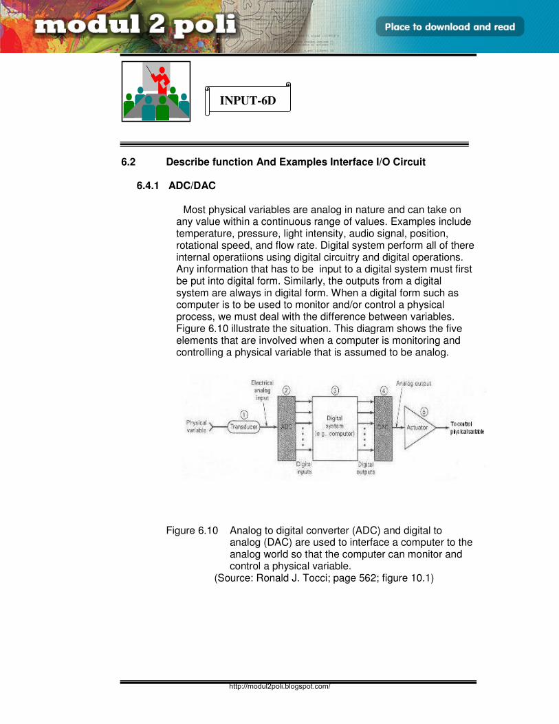
E3165 / UNIT / 26
INPUT/OUTPUT AND INTERFACE
6.2 Describe function And Examples Interface I/O Circuit
6.4.1 ADC/DAC
Most physical variables are analog in nature and can take on any value within a continuous range of values. Examples include temperature, pressure, light intensity, audio signal, position, rotational speed, and flow rate. Digital system perform all of there internal operatiions using digital circuitry and digital operations. Any information that has to be input to a digital system must first be put into digital form. Similarly, the outputs from a digital system are always in digital form. When a digital form such as computer is to be used to monitor and/or control a physical process, we must deal with the difference between variables. Figure 6.10 illustrate the situation. This diagram shows the five elements that are involved when a computer is monitoring and controlling a physical variable that is assumed to be analog.
Figure 6.10 Analog to digital converter (ADC) and digital to
analog (DAC) are used to interface a computer to the analog world so that the computer can monitor and control a physical variable.
(Source: Ronald J. Tocci; page 562; figure 10.1)
INPUT-6D
http://modul2poli.blogspot.com/
E3165 / UNIT / 27
INPUT/OUTPUT AND INTERFACE
1. Transducer. The physical variable is normally a nonelectrical quantity. A transducer is a device that converts the physical variable to an electrical variable. Some common transducer include thermistors, photocells, photodiodes, flow meter, pressure transducers, and tachnometers. The electrical output of the transducer is an analog current or voltage that is proportional to the physical variable it is monitoring. For example, the physical variable could be the temperature of a water in a large tank that is being filled from cold and hot water pipes. Let’s say that the water temperature varies from 80 to 150 oF and that a thermistor and its associated circuitry convert this water temperature to a voltage ranging from 800 to 1500 mV. Note that transducer’s output is directly proportional to temperature, such that each 10F produces a 10 mV output. This proportionality factor was chosen for convenience.
2. Analog to digital converter (ADC). The transducer’s electrical
analog output serves as the analog input the ADC. The ADC converts this analog input to a digital output. This digital output consists of a number of a bits that represent the value of the analog input. For example, the ADC might convert 01010000 (80) to 10010110 (150). Note that the binary output from the ADC is proportional to the analog input voltage so that each unit of the digital output represent 10 mV.
3. Computer. The digital representation of the process variable is
transmitted from the ADC to the digital computer, which store the digital value and processes it according to a program of instruction that is executing. The program might perform calculations or other operation on this digital representation of temperature to come up with a digital output will eventually be used to control the temperature.
4. Digital to Analog Converter (DAC). This this digital output form
the computer is connected to a DAC, which convert it to a proportional analog voltage or current. For example the computer might produce a digital output ranging from 00000000 to 11111111, which the DAC converts to a voltage ranging from 0 to 10 v.
5. Actuator. The analog signal from the DAC is often connected
to some device or circuit that serves as an actuator to control the physical variable. For our water temperature example, the actuator might be an electrically conrolled valve that regulates the flow of hot water into the tack in accordance with the analog voltage from the DAC. The flow rate would vary in proportion to this analog voltage, with 0v producing no flow and 10 v producing the maximum flow rate.
http://modul2poli.blogspot.com/
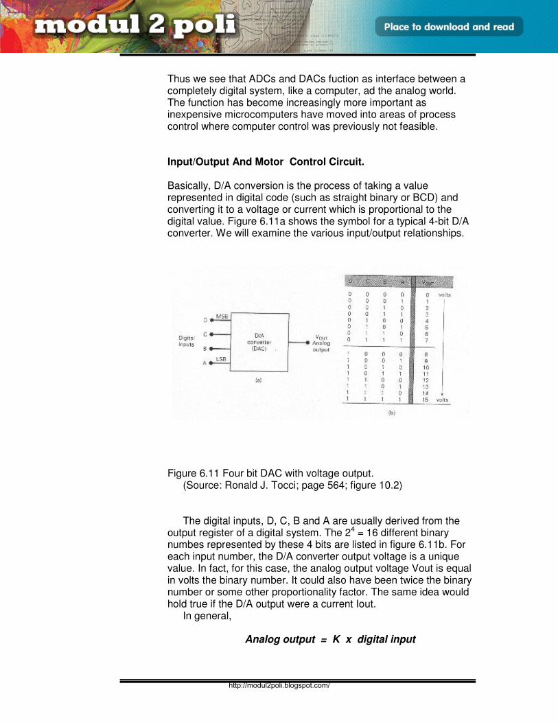
E3165 / UNIT / 28
INPUT/OUTPUT AND INTERFACE
Thus we see that ADCs and DACs fuction as interface between a completely digital system, like a computer, ad the analog world. The function has become increasingly more important as inexpensive microcomputers have moved into areas of process control where computer control was previously not feasible. Input/Output And Motor Control Circuit. Basically, D/A conversion is the process of taking a value represented in digital code (such as straight binary or BCD) and converting it to a voltage or current which is proportional to the digital value. Figure 6.11a shows the symbol for a typical 4-bit D/A converter. We will examine the various input/output relationships.
Figure 6.11 Four bit DAC with voltage output.
(Source: Ronald J. Tocci; page 564; figure 10.2) The digital inputs, D, C, B and A are usually derived from the output register of a digital system. The 24 = 16 different binary numbes represented by these 4 bits are listed in figure 6.11b. For each input number, the D/A converter output voltage is a unique value. In fact, for this case, the analog output voltage Vout is equal in volts the binary number. It could also have been twice the binary number or some other proportionality factor. The same idea would hold true if the D/A output were a current Iout. In general, Analog output = K x digital input
http://modul2poli.blogspot.com/
E3165 / UNIT / 29
INPUT/OUTPUT AND INTERFACE
Where K is the proportionality factor and is a constant value for a given DAC. The anaog can of course be a voltage or current. When it is a voltage, k will be in voltage units, and when the output is current, k wil be in current units. For the DAC of figure 6.12, K = 1v, so that Vout = ( 1 v ) X digital input We can use this to calculate Vout for any value of digital input. For example, with a digital input of 11002 = 1210 we obtain Vout = 1 v X 12 = 12 v
Example A 5 bit Dac has a current output. For a digital input of
10100, an output current of 10 mA is produced. What will I out be for a digital input of 11101?
Solution The digital input 101002 is equal to decimal 20. Since
Iout =m 10 mA for this case, the proportionality factor must be 0.5 mA. Thus we can find Iout for any digital input such as 111012 = 2910 as follows;
Iout = (0.5 mA ) x 29 = 14.5 mA remember, the proportionality factor, k will vary from 1one DAC
to another
http://modul2poli.blogspot.com/
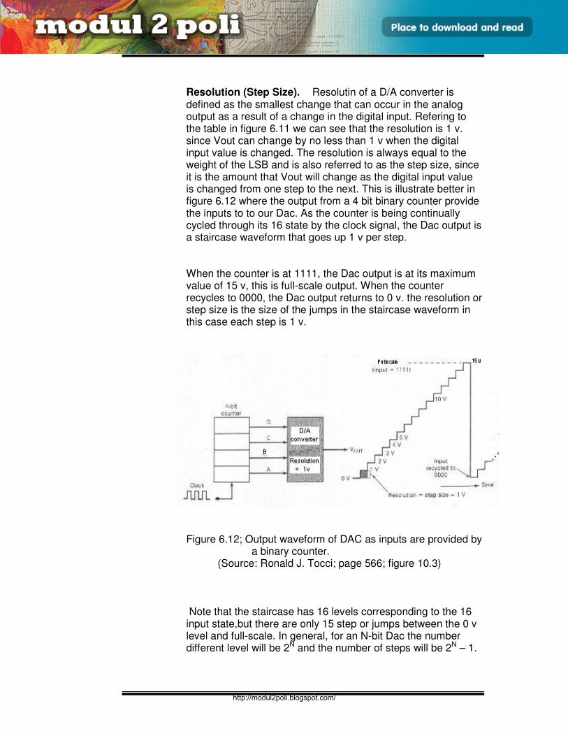
E3165 / UNIT / 30
INPUT/OUTPUT AND INTERFACE
Resolution (Step Size). Resolutin of a D/A converter is
defined as the smallest change that can occur in the analog output as a result of a change in the digital input. Refering to the table in figure 6.11 we can see that the resolution is 1 v. since Vout can change by no less than 1 v when the digital input value is changed. The resolution is always equal to the weight of the LSB and is also referred to as the step size, since it is the amount that Vout will change as the digital input value is changed from one step to the next. This is illustrate better in figure 6.12 where the output from a 4 bit binary counter provide the inputs to to our Dac. As the counter is being continually cycled through its 16 state by the clock signal, the Dac output is a staircase waveform that goes up 1 v per step.
When the counter is at 1111, the Dac output is at its maximum value of 15 v, this is full-scale output. When the counter recycles to 0000, the Dac output returns to 0 v. the resolution or step size is the size of the jumps in the staircase waveform in this case each step is 1 v.
Figure 6.12; Output waveform of DAC as inputs are provided by a binary counter. (Source: Ronald J. Tocci; page 566; figure 10.3)
Note that the staircase has 16 levels corresponding to the 16 input state,but there are only 15 step or jumps between the 0 v level and full-scale. In general, for an N-bit Dac the number different level will be 2N and the number of steps will be 2N – 1.
http://modul2poli.blogspot.com/
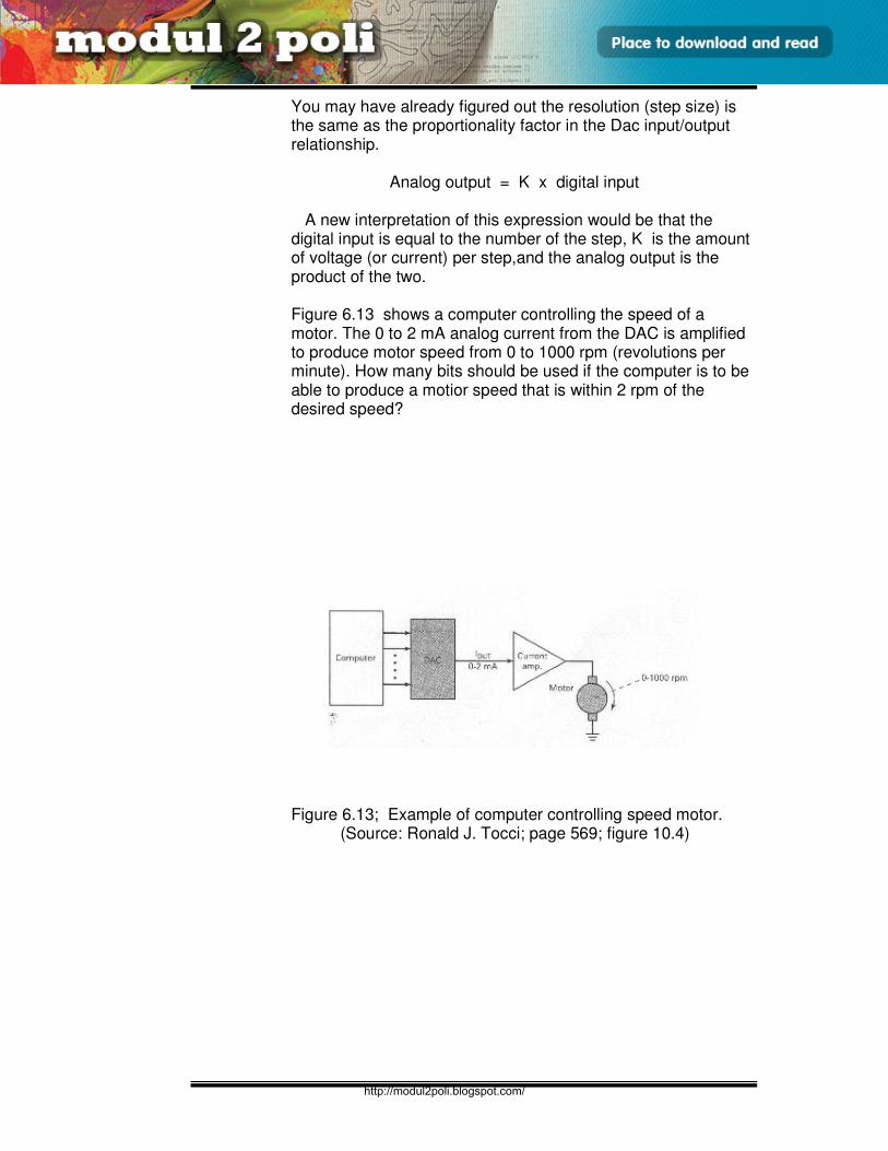
E3165 / UNIT / 31
INPUT/OUTPUT AND INTERFACE
You may have already figured out the resolution (step size) is the same as the proportionality factor in the Dac input/output relationship. Analog output = K x digital input A new interpretation of this expression would be that the digital input is equal to the number of the step, K is the amount of voltage (or current) per step,and the analog output is the product of the two. Figure 6.13 shows a computer controlling the speed of a motor. The 0 to 2 mA analog current from the DAC is amplified to produce motor speed from 0 to 1000 rpm (revolutions per minute). How many bits should be used if the computer is to be able to produce a motior speed that is within 2 rpm of the desired speed?
Figure 6.13; Example of computer controlling speed motor.
(Source: Ronald J. Tocci; page 569; figure 10.4)
http://modul2poli.blogspot.com/
E3165 / UNIT / 32
INPUT/OUTPUT AND INTERFACE
Solution
The motor speed will range from 0 to 1000 rpm as the DAC
goes from zero to full scale. Each step in the DAC output will produce a step in the motor speed. We want the step size to be no greater than 2 rpm. Thus we need at least 500 steps (1000/2). Now we must determine how many bits are required so that there are at least 500 steps from zero to full scale. We know that the number of steps is 2N – 1, and so we can say
2N - 1 ≥ 500 or
2N - 1 ≥ 501
since 28 = 256 and 29 = 512, the smallest number of bits that will produce at least 500 steps in nine. We could use more than 9 bits, but this might add the cost of the DAC.
http://modul2poli.blogspot.com/

E3165 / UNIT / 33
INPUT/OUTPUT AND INTERFACE
6D-1. Why do the analog form/value need to be converted to digital form? 6D-3. What is transducer in ADC/DAC?
6D-4. Briefly describe Actuator
6D-5 Define K in DAC?.
6D-6. Using the analog output formula,assuming K 1v, what is the Vout for
digital input 0110?
ACTIVITY – 6D
TEST YOUR UNDERSTANDING BEFORE YOU CONTINUE TO THE NEXT INPUT….!
http://modul2poli.blogspot.com/
E3165 / UNIT / 34
INPUT/OUTPUT AND INTERFACE
6D-1. Why do the analog form/value need to be converted to digital form?
Digital system perform all of there internal operatiions using digital circuitry and digital operations. Any information that has to be inputted to a digital system must first be put into digital form.
6D-3. what is transducer in ADC/DAC?
The physical variable is normally a nonelectrical quantity. A transducer is a device that converts the physical variable to an elevtrical variable
6D-4. Briefly describe Actuator
The analog signal from the DAC is often connected to some device or circuit that serves as an actuator to control the physical variable.
6D-5 Define K in DAC?. K is the proportionality factor and is a constant value for a given DAC
6D-6. Using the analog output formula,assuming K 1v, what is the Vout for
digital input 0110?
V out = 1 v X 6 ( 0110 ) = 6 v.
FEEDBACK TO ACTIVITY – 6D
http://modul2poli.blogspot.com/
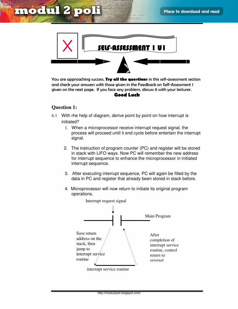
E3165 / UNIT / 35
INPUT/OUTPUT AND INTERFACE
You are approaching success. Try all the questions in this self-assessment section
and check your answers with those given in the Feedback on Self-Assessment 1 given on the next page. If you face any problem, discuss it with your lecturer.
Good Luck
Question 1:
6.1 With rhe help of diagram, derive point by point on how interrupt is
initiated?
1. When a microprocessor receive interrupt request signal, the process will proceed until it end cycle before entertain the interrupt signal.
2. The instruction of program counter (PC) and register will be stored
in stack with LIFO ways. Now PC will remember the new address for interrupt sequence to enhance the microprocessor in initiated interrupt sequence.
3. After executing interrupt sequence, PC will again be filled by the
data in PC and register that already been stored in stack before.
4. Microprocessor will now return to initiate its original program operations.
SELFSELFSELFSELF----ASSESSMENT 1 U1ASSESSMENT 1 U1ASSESSMENT 1 U1ASSESSMENT 1 U1
Interrupt request signal
Main Program
Save return
address on thestack, then
jump tointerrupt service
routine
interrupt service routine
After
completion of
interrupt service
routine, control
return to
original
http://modul2poli.blogspot.com/
E3165 / UNIT / 36
INPUT/OUTPUT AND INTERFACE
6.2 Explain what is an exchange of control signal between the microprocessor and peripheral .
• If there is to be input to the microprocessor, the peripheral first signal it is ready to send the data. The microprocessor than signals that it is ready to receive the data. The transfer goes ahead. Having received the data, the microprocessor signals the peripheral that the transfer is complete.
• If there is to be output from the microprocessor, the peripheral first signals that data are available. The data are transferred. When the transfers are complete, the peripheral signals the microprocessor
6.3 In digital data transferring, explain what is serial data transfer with the
help of a diagram
- Binary data been transfer in one line, one bit at a time.
- Transfering data are slow. - Usually used for trank data transfer, example if
microprocessor been connected to peripheral telephone line.
Computer
A
Computer B Series technique
of transfer
http://modul2poli.blogspot.com/
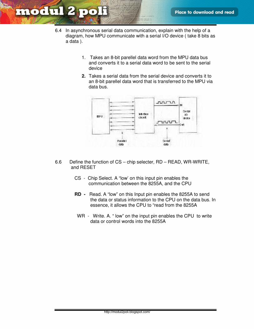
E3165 / UNIT / 37
INPUT/OUTPUT AND INTERFACE
6.4 In asynchronous serial data communication, explain with the help of a diagram, how MPU communicate with a serial I/O device ( take 8 bits as a data ).
1. Takes an 8-bit parellel data word from the MPU data bus and converts it to a serial data word to be sent to the serial device
2. Takes a serial data from the serial device and converts it to an 8-bit parellel data word that is transferred to the MPU via data bus.
6.6 Define the function of CS – chip selecter, RD – READ, WR-WRITE,
and RESET
CS - Chip Select. A “low’ on this input pin enables the communication between the 8255A, and the CPU
RD - Read. A “low” on this Input pin enables the 8255A to send
the data or status information to the CPU on the data bus. In essence, it allows the CPU to “read from the 8255A
WR - Write. A. “ low” on the input pin enables the CPU to write
data or control words into the 8255A
http://modul2poli.blogspot.com/
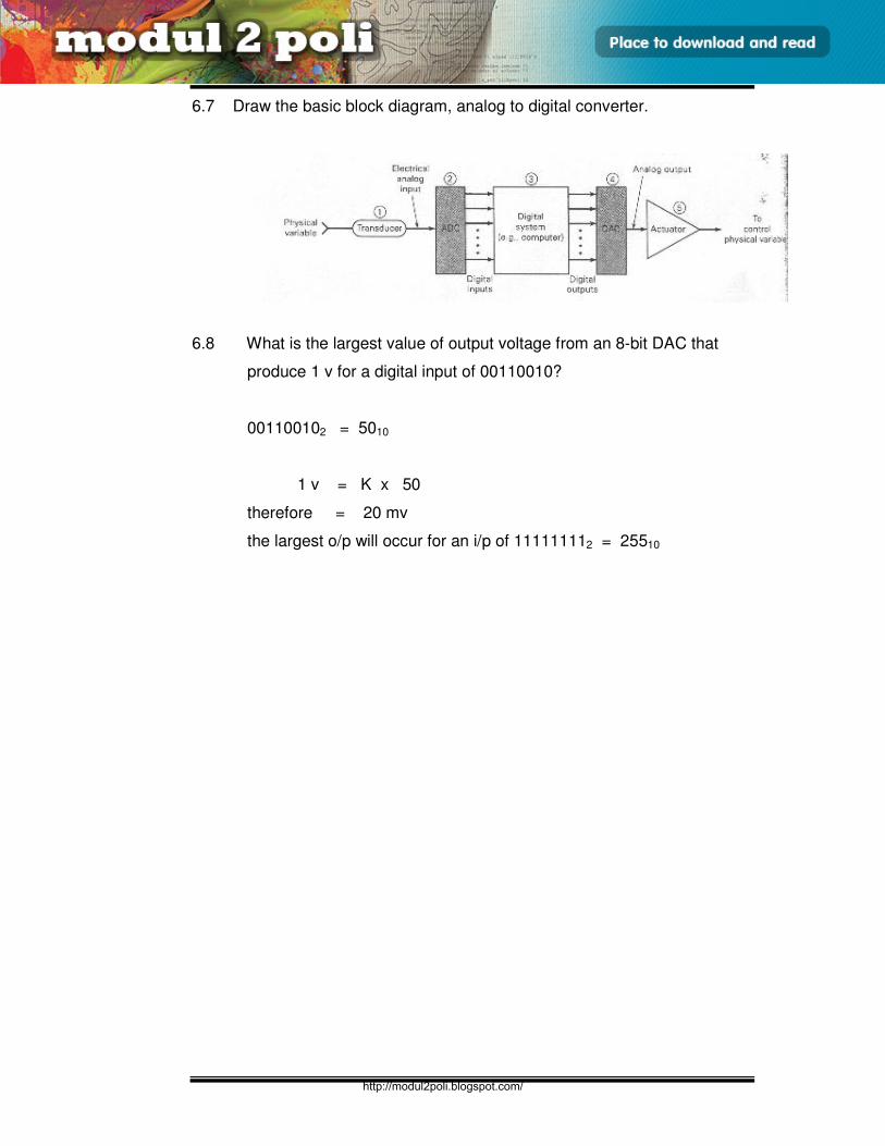
E3165 / UNIT / 38
INPUT/OUTPUT AND INTERFACE
6.7 Draw the basic block diagram, analog to digital converter.
6.8 What is the largest value of output voltage from an 8-bit DAC that
produce 1 v for a digital input of 00110010?
001100102 = 5010
1 v = K x 50
therefore = 20 mv
the largest o/p will occur for an i/p of 111111112 = 25510
http://modul2poli.blogspot.com/