PERPUSTAKAAN KUiTTHO - Institutional...
24
Transcript of PERPUSTAKAAN KUiTTHO - Institutional...

PERPUSTAKAAN KUiTTHO
11111111111111111111111111111111111111111111111111111111 111\ 3 0000 00180727 6
KOLEJ UNIVERSITI TEKNOLOGI TUN HUSSEIN ONN
BORANG PENGESAHAN STATUS TESIS·
JUDUL:
Saya
AN EXPERIMENT A L VERI FICA TION OF THE BINA RV METHOD FOR THREE-PHASE VOLTAGE SOURCE INVERTER
SESI PENGAJIAN: 2004/2005 PANG SHEN VEE (HURUF BESAR)
mengaku membenarkan tesis (PSM/SarjanalOokto[ Falsafah)* ini disimpan di Perpustakaan dengan syarat-syarat kegunaan seperti berikut:
I. Tesis adalah hakmilik Kolej Universiti Teknologi Tun Hussein ann. 2. Perpustakaan dibenarkan membuat salinan untuk tujuan pengajian sahaja. 3. Perpustakaan dibenarkan membuat salinan tesis ini sabagai pertukaran antara institusi
pengajian tinggi. 4. **Sila tandakan (,!')
D SULIT (Mengandungi maklumat yang berdarjah keselamatan atau kepentingan Malaysia seperti yang termaktub di dalam (AKT A RAHSIA RASMI 1972)
D TERHAD (Mengandungi maklumat TERHAD yang telah ditentukan oleh organisasilbadan di mana penyelidikan dijalankan)
Q TIDAK TERHAD Disahkan oleh;
0i~tk . d~~ (TANDA T A N.P't!ENYELIA) (TANDATANGAN PENULlS)
Alamat tetap: 88, SITE B, I,ORONG 2 4')400 SEKINCHAN SEI,ANGOE
PROF DR HASHIM BIN SAIM Nama Penyelia
Tarikh: 31MAC 2005 Tarikh: 31MAC 2005
CATATAN: * Potong yang tidak berkenaan. ** Jib tcsis ini SULIT at au TERHAD, sila lampirkan surat daripada pihak
bcrkuasalorganisasi bcrkcnaan dcngan mcnyatakan sckali scbab dan tcmpoh tcsis ini pcrlu dikclaskan scbagai SULIT atau TERHAD.
• Tcsis dimaksudkan scbagai tcsis bagi Ijazah Doktor Falsafah dan Sarjana sccara pcnyclidikan, atau discrtasi bagi pcngajian sccara kcrja kursus dan pcnyclidikan, atau Laporan Projck Sarjana Muda (PSM).
"SayttlKami akui bahawa s-ayaIkami telah membaca karya ini dan pada pandangan
s-ayaIkami karya ini adalah memadai dari segi skop dan kualiti untuk tujuan
penganugerahan Ijazah Sarjana Kejuruteraan (Elektrikal)."
Tandatangan
Nama Penyelia I
Tarikh
Tandatangan
Nama Penyelia II
Tarikh
Tandatangan
Nama Penyelia III
Tarikh
: .... 3JM.<,l~ .2.Q.Q~ ............................ .
: ............ M ...................... . : . .J:!~9f~?9~ .I0.'!-~y.? .J:!m~g .<;:;h~. f. R~g. : .... 3.1M.<,l~ .2.Q.Q~ ............................ .
: .. , P!-!?\Q .. ~QR~ .Gh~~ . .f:h9ng ... , ....... . .. ).1.M~.<;)O.O.~ ............................ .
AN EXPERIMENTAL VERIFICATION OF THE BINARY METHOD FOR
THREE-PHASE VOLTAGE SOURCE INVERTER
PANG SHEN YEE
A thesis submitted
in fulfillment of the requirements for the award of the
Degree of Master of Engineering (Electrical)
Faculty of Electrical and Electronic Engineering
Kolej Universiti Teknologi Tun Hussein Onn
MARCH, 2005

11
"The author hereby declares that no part of the study was covered by copyright.
All the information, quotations and excerpts from other references are well stated.
Otherwise the rest of the information presented through this study is a sole work and
experimentally carried out by the author"
Signature . nr1V(\~l 0 - . •
.......... !J. .... y .......... . Author : ... PAND. SHEN .Y.E.B. ....
Date : .... ;3JM~.r.~b.2.QO.~ ......... .

Especially for grandmum, parents, brothers
and Hong Wai with love
III

IV
ACKNOWLEDGEMENT
First and foremost, I would like to express my genuine gratitude to my supervisor
Professor Dr. Hashim Bin Saim, my co-supervisor Associate Professor Pang Che Fong
and Madam Soon Chin Fhong. Because of their professional guidance and valuable
advice, I could achieve the goal of this project.
I am truly indebted those who assist me along the period of this project especially
En.Zaihan from Power Electronics Laboratory and En. Khairul from PCB Laboratory. By
taking this chance, I wish to accolade Lynn Schauer, Don Lancaster and many others who
give me the inspirational idea and opinion.
Last but not least, I would like to express my wholehearted gratefulness to my
beloved family and friends, for their unconditional support and encouragement
v
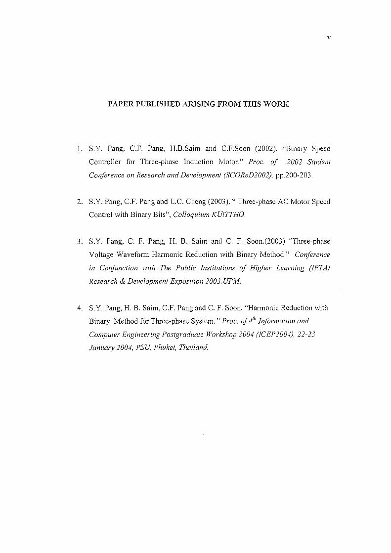
PAPER PUBLISHED ARISING FROM THIS WORK
1. S.Y. Pang, C.F. Pang, H.B.Saim and C.F.Soon (2002). "Binary Speed
Controller for Three-phase Induction Motor." Proc. of 2002 Student
Conference on Research and Development (SCOReD2002). pp.200-203.
2. S.Y. Pang, C.F. Pang and L.C. Cheng (2003). " Three-phase AC Motor Speed
Control with Binary Bits", Colloquium KUiTTHO.
3. S.Y. Pang, C. F. Pang, H. B. Saim and C. F. Soon.(2003) "Three-phase
Voltage Waveform Harmonic Reduction with Binary Method." Conference
in Conjunction with The Public Institutions of Higher Learning (IPTA)
Research & Development Exposition 2003, UP M.
4. S.Y. Pang, H. B. Saim, C.F. Pang and C. F. Soon. "Harmonic Reduction with
Binary Method for Three-phase System. " Proc. of 4'" Information and
Computer Engineering Postgraduate Workshop 2004 (ICEP2004), 22-23
January 2004, PSU, Phuket, Thailand.
VI
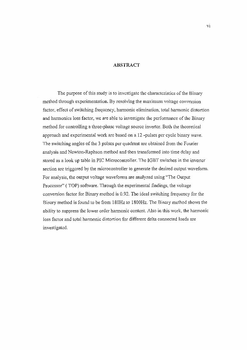
ABSTRACT
The purpose of this study is to investigate the characteristics of the Binary
method through experimentation. By resolving the maximum voltage conversion
factor, effect of switching frequency, harmonic elimination, total harmonic distortion
and harmonics loss factor, we are able to investigate the performance of the Binary
method for controlling a three-phase voltage source inverter. Both the theoretical
approach and experimental work are based on a 12 -pulses per cycle binary wave.
The switching angles of the 3 pulses per quadrant are obtained from the Fourier
analysis and Newton-Raphson method and then transformed into time delay and
stored as a look up table in PIC Microcontroller. The IGBT switches in the inverter
section are triggered by the microcontroller to generate the desired output waveform.
For analysis, the output voltage waveforms are analyzed using "The Output
Processor" ( TOP) software. Through the experimental findings, the voltage
conversion factor for Binary method is 0.92. The ideal switching frequency for the
Binary method is found to be from 180Hz to 1800Hz. The Binary method shows the
ability to suppress the lower order harmonic content. Also in this work, the harmonic
loss factor and total harmonic distortion for different delta connected loads are
investigated.
VII
ABSTRAK
Tujuan kajian ini adalah untuk menyelidik ciri-ciri kaedah Binari melalui
kaedah ujikaji. Dengan mengetahui faktor penukaran voltan maksimum, kesan
frekuensi pensuisan, penghapusan harrnonik, hero tan harrnonik keseluruhan dan
faktor kehilangan harrnonik, pre stasi kaedah Binari dalam mengawal penyongsang
punca voltan tiga-fasa dapat dikenalpasti. Kedua-dua kaedah pendekatan teori dan
ujikaji adalah berdasarkan kepada gelombang binari 12 denyut per kitar. Sudut
sudut pensuisan 3 denyut per suku kitar dapat ditentukan melalui anal isis Fourier and
kaedah Newton-Raphson. Kemudian, sudut-sudut pensuisan ini ditukar kepada masa
lengah dan disimpan dalam ingatan pengawal mikro PIC melalui kaedah
penjadualan. Suis IGBT yang berada pada bahagian penyongsang dipicu oleh
pengawal mikro supaya menghasilkan gelombang keluaran yang diingini.
Gelombang voltan keluaran dianalisis oleh perisian pemproses keluaran (TOP).
Faktor penukaran voltan maksimum hasil daripada ujikaji bagi kaedah Binari adalah
0.92 . Kaedah Binari mempunyai frekuensi pensuisan unggul yang berada dalam
lingkungan 180Hz ke 1800Hz. Selain daripada itu, kaedah Binari menunj ukkan
keupayaannya untuk menindaskan kandungan harmonik tertib rendah. Faktor
kehilangan harrnonik dan herotan harrnonik keseluruhan untuk pelbagai beban yang
disambung secara delta juga diperolehi melalui ujikaji yang dijalankan.
CHAPTER
TITLE PAGE
TESTIMONY
DEDICATION.
ACKNOWLEDGEMENT
CONTENTS
ITEM
PAPER PUBLISHED ARISING FROM THIS WORK
ABSTRACT
ABSTRAK
CONTENTS
PAGE
11
111
IV
V
VI
Vll
Vlll
Xl
xiii
VlIl
LIST OF TABLES
LIST OF FIGURES
LIST OF SYMBOLS
LIST OF ABBREVIATIONS
LIST OF APPENDICES
XVI
xviii
I INTRODUCTION
l.1 Introduction
l.2 Problem Statement
l.3 Objectives
1.4 Scope of Study
l.5 Organization of Thesis
XIX
3
4
4
6
II AN OVERVIEW OF BINARY METHOD
2.1 Introduction 7
2.2 Single-phase Binary Sine Waves 8
2.2.1 Choosing Binary Combination of Ones and Zeros 10
IX
2.2.2 Mathematical Fonnulation 14
2.3 Delta Friendly Three-phase Binary Waves 15
2.4 Summary 21
III RESEARCH METHODOLOGY
3.1 Introduction 23
3.2 Binary Method Approach 24
3.2.1 Generating Binary Wavefonn By Ones and Zeros 24
3.2.2 Samples of Binary Selection 26
3.2.3 Newton-Raphson Numerical Method 27
3.2.4 Three-phase Binary Wavefonn Selection 30
3.3 PIC Microcontroller Timing Calculation 34
3.3.1 Program Flow Chart and Description 38
3.4 Hardware Implementation 44
3.4.1 PIC Circuit Connection 44
3.4.2 Gate Driver Circuit 46
3.4.3 Three-phase Inverter Circuit 49
3.5 Analysis Software 51
3.5.1 TOP Software 51
3.6 Experiment Overview 52
3.6.1 Perfonnance Indices 55
3.6.2 Limitations 57
3.7 Summary 58
IV RESULTS AND DISCUSSION
4.1 Introduction 59
4.2 Result of Zeros and Ones Combinations 59
4.2.1 6-bit per quadrant sequence 60
4.2.2 9-bit per quadrant sequence 60
4.2.3 12-bit per quadrant sequence 61
4.2.4 IS-bit per quadrant sequence 62
4.2.5 18-bit per quadrant sequence
4.2.6 21-bit per quadrant sequence
4.2.7 24-bit per quadrant sequence
4.2.8 Discussion
4.3 Results of Three-phase Binary Wavefonn Calculations
4.3.1 Relationship of Switching Angles and Amplitude
4.3.2 Relationship of Delay versus Amplitude
4.4 Experimental Results
4.4.1 Voltage Conversion Factor
4.4.2 Effect of Switching Frequency
4.4.3 Hannonic Analysis and FFT Display
4.4.4 Total Hannonic Distortion
4.4.5 Hannonic Loss Factor
4.5 Summary
V CONCLUSIONS AND RECOMMENDATIONS FOR FUTURE
WORK
5.1 Conclusions
5.2 Recommendations for Future Work
REFERENCES
APPENDIX A-H
x
63
64
64
65
67
70
71
72
73
78
81
88
89
91
93
94
95
100
Xl
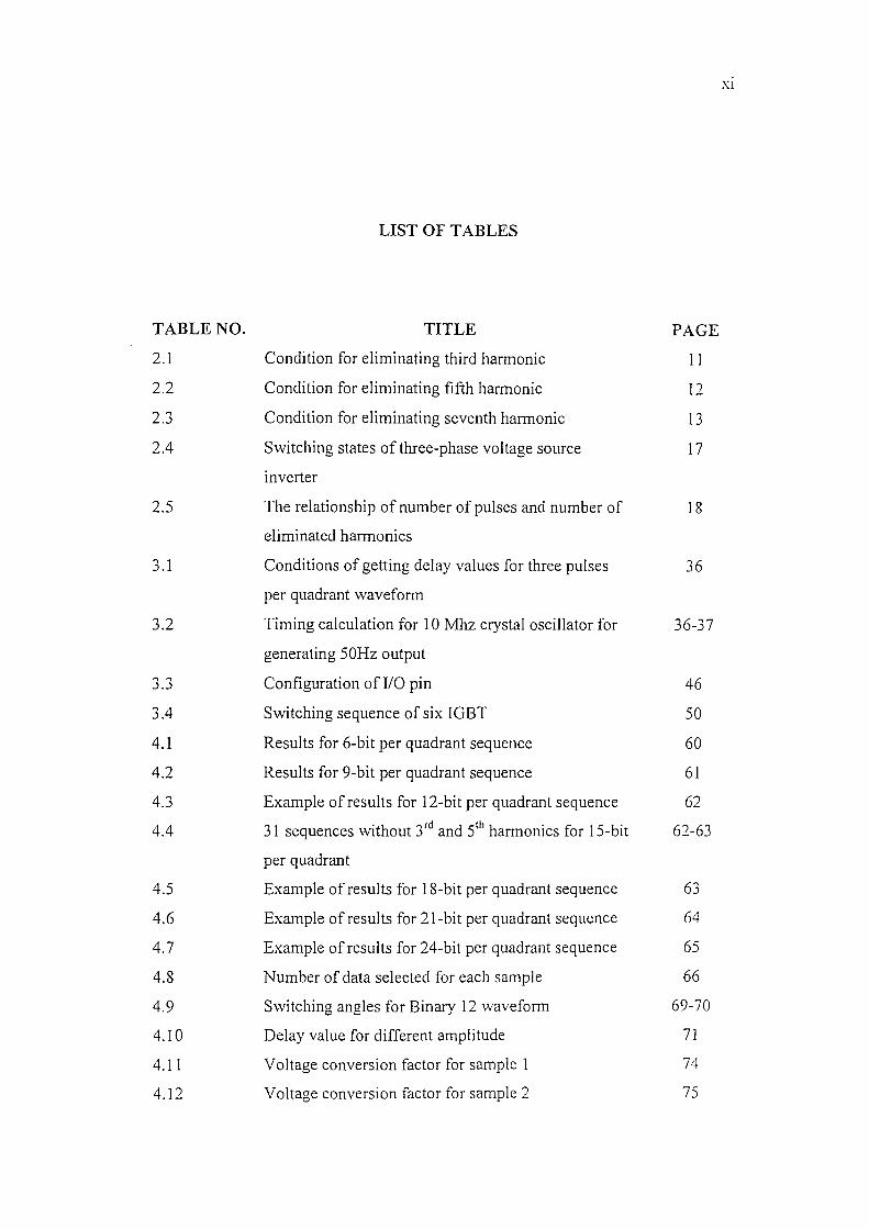
LIST OF TABLES
TABLE NO. TITLE PAGE
2.1 Condition for eliminating third harmonic 1 I
2.2 Condition for eliminating fifth harmonic 12
2.3 Condition for eliminating seventh harmonic 13
2.4 Switching states of three-phase voltage source 17
inverter
2.5 The relationship of number of pulses and number of 18
eliminated harmonics
3.1 Conditions of getting delay values for three pulses 36
per quadrant waveform
3.2 Timing calculation for 10 Mhz crystal oscillator for 36-37
generating 50Hz output
3.3 Configuration of VO pin 46
3.4 Switching sequence of six IGBT 50
4.1 Results for 6-bit per quadrant sequence 60
4.2 Results for 9-bit per quadrant sequence 61
4.3 Example of results for l2-bit per quadrant sequence 62
4.4 31 sequences without 3 rd and 5th harmonics for IS-bit 62-63
per quadrant
4.5 Example of results for 18-bit per quadrant sequence 63
4.6 Example of results for 2l-bit per quadrant sequence 64
4.7 Example of results for 24-bit per quadrant sequence 65
4.8 Number of data selected for each sample 66
4.9 Switching angles for Binary 12 waveform 69-70
4.10 Delay value for different amplitude 71
4.11 Voltage conversion factor for sample 1 74
4.12 Voltage conversion factor for sample 2 75

XlI
4.13 Voltage conversion factor for sample 3 76
4.14 Input and output phase voltage for different switching 79
frequency
4.15 Magnitude of harmonic for load 470 ohm 82
4.16 Magnitude of harmonic for load 470 ohm,1 OOmH 85
Xlll
LIST OF FIGURES
FIGURE NO. TITLE PAGE
2.l Square wave is building up by many harmonics 9
waveform
2.2 30-bit waveform and harmonics for single-phase 9
binary sine wave
2.3 % cycle of third harmonic in quarter waveform 10
2.4 1 V4 cycle of fifth harmonic in quarter waveform 12
2.5 1 3i4 cycle of seventh harmonic in quarter waveform 13
2.6 Three-phase line to neutral voltage waveforms 16
2.7 (a) Delta connection and 17
(b) Wye connection
2.8 The arrangement of three pulses per quadrant 19
2.9 The sequence of phase a, band c in a 12 pulses per 21
cycle waveform
3.1 Stage of experimental works 23
3.2 3 pulses per quadrant waveform 30
3.3 Eliminate triad harmonics with pulse positioning, 31
X-60
3.4 Eliminate triad harmonics with pulse positioning, 31
120-X
3.5 Guess and Try Program for three-phase binary 33
waveform
3.6 Programming flow chart for PIC microcontroller 38
3.7 Block diagram of inverter system 44
3.8 PIC circuit connection 45
3.9 PIC microcontroller board 45
3.10 Configuration of HCPL 3150 driver 47
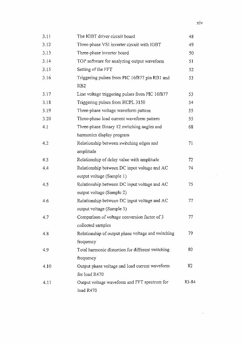
XIV
3.11 The IGBT driver circuit board 48
3.12 Three-phase VSI inverter circuit with IGBT 49
3.13 Three-phase inverter board 50
3.14 TOP software for analyzing output waveform 51
3.15 Setting of the FFT 52
3.16 Triggering pulses from PIC 16f877 pin RBI and 53
RB2
3.17 Line voltage triggering pulses from PIC 16f877 53
3.18 Triggering pulses from HCPL 3150 54
3.19 Three-phase voltage waveform pattern 55
3.20 Three-phase load current waveform pattern 55
4.1 Three-phase Binary 12 switching angles and 68
harmonics display program
4.2 Relationship between switching edges and 71
amplitude
4.3 Relationship of delay value with amplitude 72
4.4 Relationship between DC input voltage and AC 74
output voltage (Sample 1)
4.5 Relationship between DC input voltage and AC 75
output voltage (Sample 2)
4.6 Relationship between DC input voltage and AC 77
output voltage (Sample 3)
4.7 Comparison of voltage conversion factor of 3 77
collected samples
4.8 Relationship of output phase voltage and switching 79
frequency
4.9 Total harmonic distortion for different switching 80
frequency
4.10 Output phase voltage and load current waveform 82
for load R470
4.11 Output voltage waveform and FFT spectrum for 83-84
load R470

xv
4.12 Output phase voltage and load current waveform 85
for load R470, L100mH
4.13 Output voltage waveform and FFT spectrum for 86-87
load R470
4.l4 Total harmonic distortion for different load 89
4.15 Harmonic loss factor for various loads 90
XVI
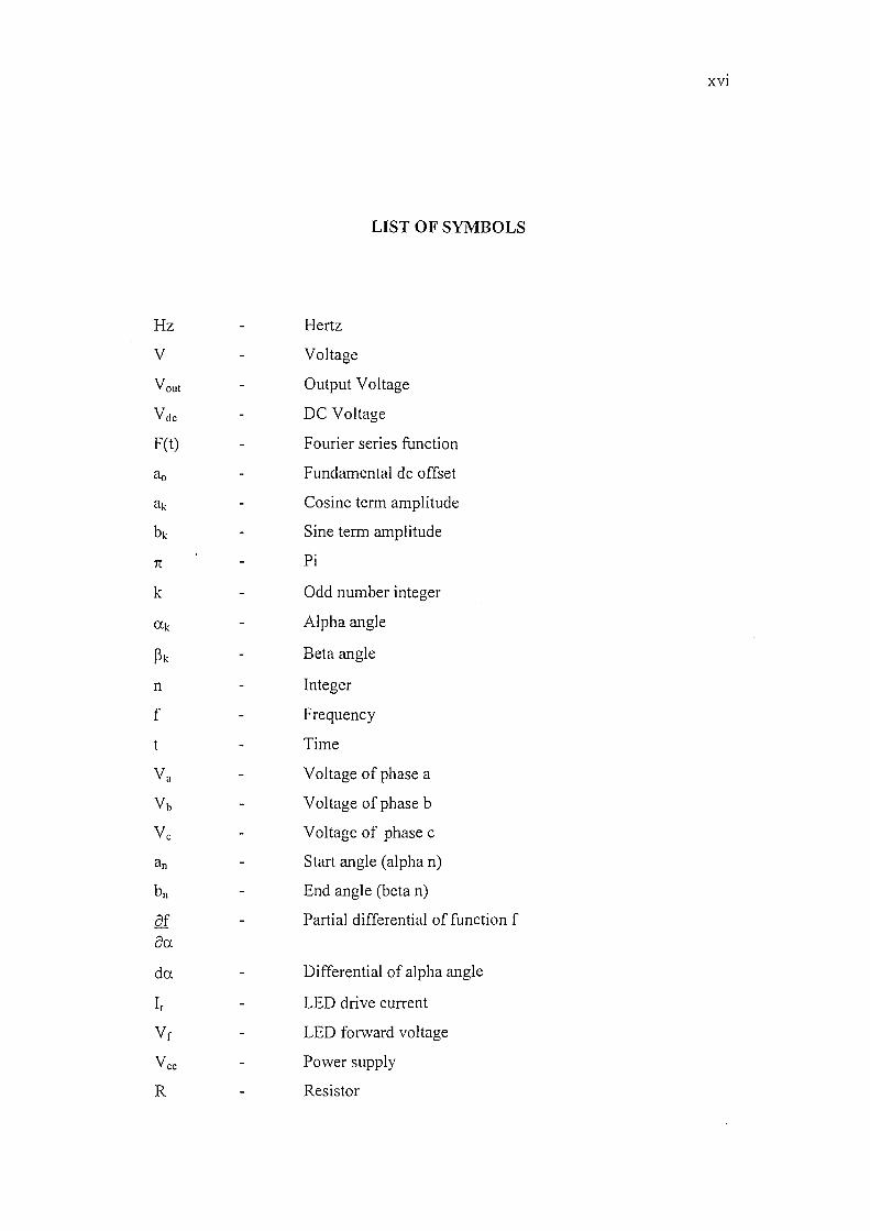
LIST OF SYMBOLS
Hz Hertz
V Voltage
Vout Output Voltage
Vde DC Voltage
F(t) Fourier series function
aa Fundamental dc offset
ak Cosine term amplitude
bk Sine term amplitude
11: Pi
k Odd number integer
Uk Alpha angle
~k Beta angle
n Integer
f Frequency
t Time
Va Voltage of phase a
Vb Voltage of phase b
Ve Voltage of phase c
an Start angle (alpha n)
bn End angle (beta n)
af Partial differential of function f
au du Differential of alpha angle
Ir LED drive current
Vr LED forward voltage
Vee Power supply
R Resistor

L
c
V ph-ph
VI
Vn
Inductor
Output conversion factor
Phase to phase voltage
Fundamental voltage (rms)
Magnitude of nth harmonic
X\'II
AC
DC
PWM
THD
IGBT
HEPWM
SPWM
ANN
TLN
TLL
EPROM
VSI
PC
FFT
LED
VB
TOP
rms
HLF
LIST OF ABBREVIATIONS
Alternative Current
Direct Current
Pulse Width Modulation
Total Harmonic Distortion
Insulated Gate Bipolar Transistor
Harmonic Elimination Pulse Width Modulation
Sinusoidal Pulse Width Modulation
Artificial Neural Network
Three-phase Line to Neutral
Three-phase Line to Line
Electrically Programmable Read Only Memory
Voltage Source Inverter
Personal Computer
Fast Fourier Transform
Light Emitted Diode
Visual Basic Programming
The Output Processor
Root Mean Square
Harmonic Loss Factor
XVlll
XIX
LIST OF APPENDICES
APPENDIX TITLE PAGE
A Newton-Raphson method in Matlab 100
B Guess and Try Program 101
C Binary Method Source Code 105
D PIC Microcontroller 116
E TOP Software 120
F Three-phase Binary Switching Angles 125
G Samples of different switching frequency for 152
amplitude scale 1.0
H The selected samples for different load with 157
switching frequency of scale 50 (300Hz)
CHAPTER I
INTRODUCTION
1.1 Introduction
The application of semiconductor devices in the electrical power field has
been increasing tremendously since the past few decades [1-4]. The power converters
make it possible to deliver high performance and low cost drives for wide range of
commercial, vehicular, military and residential applications. Hence, the converter
systems contribute to efficient operation of electric power systems and enhance the
efficient use of electricity. As a result, it contributes much to the environmental
protection as well as energy conservation [2-3].
The application of power electronics in converters is mainly aimed for better
product quality, energy saving, compact, versatile and safer system. Rapid growth of
power electronics has been related with new power converter topology, the use of
advanced control techniques and the improvements in manufacturing [1-4]. The
voltage source inverter and current source inverter are the two most popular
topologies to convert a direct current source to an AC load of arbitrary frequency and
magnitude.
Inverter circuit plays an important role to convert the DC voltage to the AC
voltage. Throughout the inversion, the amplitude, frequency and current can be well
controlled. However, the inverter itself cannot work efficiently without good control
method.