Simulation and Characterization of Photonic Crystals as Waveguide in Microwave Regime
23
I 8 ja 60•1 116 I Ptjjeimet ik ,r• „, 11N1VERS1T1 SA1NS MA L.1Y Of T ERM, 4 sit) Sains Malaysia Aras , Bangunan Canselori UNIVERSITI SANS MALAYSIA No. Fail : F0256 Tarikh Disember 2011 Prof. Madya Mohd Zubir Mat J Timbalan Dekan (Pengajian Siswazah & Penye telik Pusat Pengajian Sains Fizik Universiti Sains Malaysia . • Pejabat Pengurusan Dan Kreativiti Penyelidikan Research Creativity and Management Office Canselori, 1180 ► , USM Pulau Pinang t T : 6)04-653 3108/3178/3988/5019 F : 6)04-656 6466/8470 _6)04-653 2350 L •www.research.usm.my Tuan, LAPORAN AKHIR SKIM GERAN PENYELIDIKAN FUNDAMENTAL (FRGS) Tajuk Projek : Simulation and Characterization of Photonic Crystals as Waveguide in Microwave Regime No. Akaun : 203/PFIZIK/671166 Dengan hormatnya perkara di atas dirujuk. Terlebih dahulu saya ucapkan ribuan terima kasih di atas satu salinan laporan akhir untuk projek penyelidikan seperti tajuk di atas. Adalah dimaklumkan walaupun projek ini telah selesai, kerjasama Jabatan Bendahari dipohon untuk menguruskan penutupan akaun projek pada selewat-lewatnya 31 Disember 2011. Tempoh ini bertujuan untuk menyelesaikan semua urusan tuntutan dan bayaran yang telah dibelanjakan di dalam tempoh projek. Walau bagaimanapun, tuan dinasihatkan supaya tidak mengeluarkan borang-borang pesanan baru di dalam tempoh ini. 4. Selanjutnya sila ambil perhatian terhadap perkara-perkara berikut sekiranya berkaitan: Semua penerbitan harus merakamkan penghargaan kepada Skim Geran Penyelidikan Fundamental (FRGS) dan tuan dipohon mengemukakan satu salinan ke Pejabat ini. Bahagian Penyelidikan & Inovasi boleh/akan mengagihkan semula peralatan yang telah dibeli menggunakan peruntukan geran ini seandainya terdapat penyelidik lain yang memerlukan peralatan tersebut. 5. Akhir sekali, tahniah di atas usaha dan kejayaan pihak tuan dapat menyelesaikan projek ini dengan jayanya. Sekian, terima kasih. "BERKHIDMAT UNTUK NEGARA" 'Memastikan Kelestarian Hari Esok' Yang T1 enjalankan tugas, HA H Sa) (AMRA 6THMAN) Penolong Pendaftar Unit Pengurusan Geran & Kontrak
-
Upload
zi-shun-kudo -
Category
Documents
-
view
32 -
download
1
Transcript of Simulation and Characterization of Photonic Crystals as Waveguide in Microwave Regime

I 8 ja60•1 116
IPtjjeimet ik,r• „,
11N1VERS1T1 SA1NS MAL.1Y
Of TERM, 4sit) Sains Malaysia
Aras , Bangunan Canselori
UNIVERSITISANSMALAYSIA
No. Fail : F0256Tarikh Disember 2011
Prof. Madya Mohd Zubir Mat JTimbalan Dekan(Pengajian Siswazah & Penye telikPusat Pengajian Sains FizikUniversiti Sains Malaysia . •
Pejabat Pengurusan Dan Kreativiti PenyelidikanResearch Creativity and Management Office
Canselori,
1180 ► , USM Pulau Pinangt T : 6)04-653 3108/3178/3988/5019
F : 6)04-656 6466/8470_6)04-653 2350
L •www.research.usm.my
Tuan,
LAPORAN AKHIR SKIM GERAN PENYELIDIKAN FUNDAMENTAL (FRGS)Tajuk Projek : Simulation and Characterization of Photonic Crystals as Waveguide
in Microwave RegimeNo. Akaun : 203/PFIZIK/671166
Dengan hormatnya perkara di atas dirujuk.
Terlebih dahulu saya ucapkan ribuan terima kasih di atas satu salinan laporan akhiruntuk projek penyelidikan seperti tajuk di atas.
Adalah dimaklumkan walaupun projek ini telah selesai, kerjasama Jabatan Bendaharidipohon untuk menguruskan penutupan akaun projek pada selewat-lewatnya 31 Disember2011. Tempoh ini bertujuan untuk menyelesaikan semua urusan tuntutan dan bayaran yangtelah dibelanjakan di dalam tempoh projek. Walau bagaimanapun, tuan dinasihatkan supayatidak mengeluarkan borang-borang pesanan baru di dalam tempoh ini.
4. Selanjutnya sila ambil perhatian terhadap perkara-perkara berikut sekiranya berkaitan:
Semua penerbitan harus merakamkan penghargaan kepada Skim Geran PenyelidikanFundamental (FRGS) dan tuan dipohon mengemukakan satu salinan ke Pejabat ini.
Bahagian Penyelidikan & Inovasi boleh/akan mengagihkan semula peralatan yang telahdibeli menggunakan peruntukan geran ini seandainya terdapat penyelidik lain yangmemerlukan peralatan tersebut.
5. Akhir sekali, tahniah di atas usaha dan kejayaan pihak tuan dapat menyelesaikan projekini dengan jayanya.
Sekian, terima kasih.
"BERKHIDMAT UNTUK NEGARA"'Memastikan Kelestarian Hari Esok'
Yang T1 enjalankan tugas,
HA H Sa)(AMRA 6THMAN)Penolong PendaftarUnit Pengurusan Geran & Kontrak

LAPORAN AKHIR SKIM GERAN PENYELIDIKAN FUNDAMENTAL (FRGS)Tajuk Projek : Simulation and Characterization of Photonic Crystals as Waveguide
in Microwave RegimeNo. Akaun : 203/PFIZIK/671166
s. k. Dekan PenyelidikanPelantar Sains FundamentalPejabat Pelantar PenyelidikanUniversiti Sains Malaysia
DekanPusat Pengajian Sains FizikUniversiti Sains Malaysia
Ketua Pustakawan</.7 - Perpustakaan Hamzah Sendut
Universiti Sains Malaysia
Penolong Bendahari KananUnit Kumpulan Wang PenyelidikanJabatan BendahariUniversiti Sains Malaysia
Pegawai SainsPelantar Sains FundamentalPejabat Pelantar PenyelidikanUniversiti Sains Malaysia
Disampaikan satu salinan laporan akhirprojek untuk simpanan Perpustakaan
Mohon kerjasama pihak puan untukmenguruskan penutupan akaun projekselewat-lewatnya pada 31 Disember2011 dan mohon kemukakan satu salinanpenyata kewangan terakhir ke Pejabat iniuntuk tujuan rekod
AO/MISFRGS IndulNaporan aktbrihrtup akaun

BORANG FRGS - P3(R) Kod Projek : I FRGS/FASA1-2009/(BIDANG)/(NAMA IPT)/(NO.RUJ. KPT)
FINAL REPORTFUNDAMENTAL RESEARCH GRANT SCHEME (FRGS)
Laporan Akhir Skim Geran Penyelidikan Asas (FRGS) IPTPindaan 1/2009
RESEARCH TITLETajuk Penyelidikan
Simulation and characterization of Photonic Crystals as Waveguide in Microwave Region
PROJECT LEADER : Prof. Madya Mohd Zubir Mat JafriKetua Projek
PROJECT MEMBERS :(including GRA)Ahli Projek
Prof. Madya Sohail Aziz KhanDr. Lim Hwee SanMr. Wong Chow JengMr. Low Khee Lam
ACHIEVEMENT PERCENTAGE
Project progress according tomilestones achieved up to thisperiod
0 - 50% 51 - 75% 76 - 100%
Percentage 95%
RESEARCH FINDINGS
booksNumber of articles/ manuscripts/
Indexed Journal [ Non-Indexed Journal
1
Paper presentationsInternational National
2 4
Others(Please specify)
HUMAN CAPITAL DEVELOPMENT
IHuman Capital
NumberOthers (Please specify):
On-going I GraduatedPhD Student 2 1
Masters Student 1 2Undergraduate Students 4Temporary Research OfficerTemporary Research Assistant-1
Total

$ f
EXPENDITURE (Perbelanjaan)
C Budget Approved (Peruntukan diluluskan) : RM 36,700.00Amount Spent (Jumlab Perbelanjaan) : RM 36,697.68
Balance (Baki) • RM 2.32Percentage of Amount Spent • %
(Peratusan Be/an/a)
InternationalActivity Date (Month, Year) Organizer
(e.g : Course/ Seminar/ Symposium/Conference/ Workshop/ SiteVisit)
NationalActivity Date (Month, Year) Organizer
(e.g : Course/ Seminar/ Symposium/Conference/ Workshop/ SiteVisit)
Masa perlanjutan dipohon dan diluluskan. Diperlukan penyelidikan mengambil lebih masa terutama untuk penerbitan diterima serta urusan bayaran PO.
Peruntukan yang lebih besar diperlukan

DateTarikh
776174:3"1
14 Sept. 2010 Project Leader's Signature:Tandatangan Ketua Projek f Mat Jot
kanPen elidtkon
Name: Signature:Nama: Tandatangan:
Date:Tarikh:
RESEARCH ABSTRACT — Not Mire Than 200 VVords(Abstrak Penyelidikan — Tidak Melebihi 200 patah perkataan)
This project is to study the fundamental characteristic of photonic crystals in microwave region. The most uniquecharacteristic of this structure is the band gap which can be observed from the band structure graph of photoniccrystals. So, we denoted the plane wave expansion method to study the band structure graph of the photonic crystals.Several materials are used to create the photonic crystals. Plane wave expansion method is modified to investigate themetals material. This is because more characteristic can be observed in metal materials compared to the conventional.We found that there is wave activities below the plasma frequency which is not occured for a conventional metalsstructure. So, we studied the effective plasma frequency of the photonic crystals.

BUKU PROFIL PENYELIDIKAN SKIM GERAN PENYELIDIKANFUNDAMENTAL (FRGS) FASA 1/2007
SIMULATION AND CHARACTERIZATION OF PHOTONIC CRYSTALSAS WAVEGUIDE IN MICROWAVE REGION
Assoc. Prof. Dr. Mohd Zubir Mat JafriAssoc. Prof. Dr. Sohail Aziz Khan
Dr. Lim Hwee SanEn. Wong Chow Jeng
En. Low Khee LamUniversiti Sains Malaysia/School of Physics
[email protected] Science
ABSTRACT (120 words)
This project is to study the fundamental characteristic of photonic crystals in microwaveregion. The most unique the character of this structure is the band gap which canobserve from the band structure graph of photonic crystals. So, we denoted the planewave expansion method to study the band structure graph of the photonic crystals.Several materials are used to create the photonic crystals. Plane wave expansionmethod is modified to investigate the metals material. Then, from the band structuregraph, we created the photonic crystals waveguide.
1. INTRODUCTION
Photonic crystals or electromagnetic band gap is a repeating construction which exhibitsuseful band rejection for electromagnetic wave. This periodic structure has been widelyused in optical application. One dimension photonic crystal is normally worked as filterfor electromagnetic wave. Two dimension and three dimension photonic crystal arenormally used for wave guide application.
Photonic crystals provide a promising tool to control the flow of light in integratedoptical devices [1]. Therefore, there is great deal of interest in developing photoniccrystals based waveguide where one can confine and effecientiy guide the light aroundsharrp corners [2-5].
The basic motivation in photonic crystal based waveguides arose when thefollowing properties of the photonic band gap material (PBG), which are essential formany applications, were considered. First, photonic crystals have the property ofreflecting the EM waves within the band gap frequencies in all directions. Second, defectstructures in which the EM wave is trapped, can be created by breaking the periodicity ofthe crystal[4] These two properties have proved that the photonic crystals may serve aswaveguide. Once the EM wave is coupled inside the guide, the trapped wave, which hasno where else to go, is guided through the opening inside the crystal. This guidingmechanism is superior to traditional waveguides which rely on total internal reflection ofthe EM waves
factor tangis usually specified.ri
n = n — =
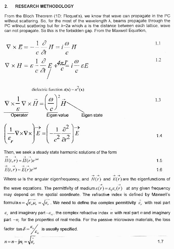
2. RESEARCH METHODOLOGY
From the Bloch Theorem (1D: Floquet's), we know that wave can propagate in the PCwithout scattering. So, for the most of the wavelength A, beams propagate through thePC without scattering but for A-2a which a is the distance between each lattice, wavecan not propagate. So this is the forbidden gap. From the Maxwell Equation,
VxE=-1 0
PI co
c
1 0 42rsV xFI =s-- E+ =i EE'cal c c
dielectric function c(x) = n 2(x)
\ 21 CO -
Vx—VxH,
Operator Eigen value Eigen state
1.1
1.2
1.3
)
VxVx E= 1.4
Then, we seek a steady state harmonic solutions of the form
H(t,r)= H(r)e-'° t 1.5-> -> - -)
E(t,r)=E(r)e' 1.6-> --> --> ->
Where w is the angular eigenfrequency, and H(r) and E(r) are the eigenfunctions of
the wave equations. The permittivity of medium g(r)= so gr (r) at any given frequency
may depend on the spatial coordinate. The refractive index is defined by Maxwell's
formula n= ‘ LinTur = . We need to define the complex permittivity c r with real part
r and imaginary part—en , the complex refractive index n with real part n and imaginary
part —n, for the properties of real media. For the passive microwave materials, the loss
1.7

2
Er = Er — jEri = n
1.8
In order to analyze the Maxwell Equation's and properties of the media, we will use thefinite difference time domain method (FDTD). To connect these field distributions to theusual circuit quantities of voltage and current, the following fundamental expressions willbe used:
gt,x,)•d1 1.9
c„
I(t,x,)= fH(t,x,)• dl 1.10
c,
where C, is a contour extending from a defined voltage reference point to the circuit xi.Similarly, contour C, to wrap completely around the strip conductor at its surface in thetransverse plane provides the load current.
For studying the loss of the photonic crystals, we will look into the scattering matrix. Fora single mode in wave guide, the transmissions and reflection methods are shown inmatrices as below:
(b1 (S11 S12 )[a] 1.11b2 SS\ 21 22 a 2
where a, b are the wave amplitudes.
al a2
Sb1
b2
To investigate the return loss, S 11 will be considered. From (2.1),
s 1.12
To investigate the insertion loss, S21 will be considered. From (2.1),
S2 = 1.13a2=0
Graph will be plotted aaain frequency.
Finally, after the computation analysis of the data, a summary on optimizing the designof the photonic crystals will be made. For this purpose, we use commercial simulationsoftware to design and optimizing the photonic crystals. The software is High FrequencyStructure Simulator. By using this software, we can design the photonic crystals we needand run a simulation on it. It will give us the return loss and insertion loss results againstfrequency. So, we will also validate our study.

25 3010 15 20wave vector
4.5
4
3.5
1
a5
0
3. LITERATURE REVIEW
Photonic crystals has been studied rigorously in this decade. First, the study was lead byYablonovitch and Sajeev [6, 7] in 1987 which they found that the periodic dielectric cancontrol the flow of light and this caused the born of photonic crystals in Physics. This isthe beginning of the photonic crystals research in the scientific area. It has become oneof the most leading researches in the world where scientists try to understand the basiccharacteristic of the photonic crystals. They used the fundamental physics of solid stateto study it. Bloch theorem, reciprocal lattice and Brillouin zones were adapted from theoriginal understanding. Due to the close relationship between periodic energy, bandstructure graph is used to describe the propagation of the wave for photonic crystals. Itcan show the stop band and propagation band of the photonic crystals. As we can see inFigure 1 an example of band structure, the shaded grey area is the stop band of thedesigned photonic crystals. Wave propagation is not allowed in this area. This isbecause the wave is destructed and there is no energy band. The entire wave is rejectedin this area and this made the very special characteristics of PC where only PC canmake it. The extensive development of solid state has opened the gate of thesemiconductor technology. It built a strong base of manipulating the currentdevelopment on the semiconductor but it was still not enough. Although scientists hadthe strong knowledge about propagation electron in solid, they are looking forward tomanipulate the light or wave in solid. This breakthrough finding will bring the new era ofinformation technology.
1 011 TE:Band structure of a 20 tri-anquiar pbatorric band structure5
Figure 1 Dispersion graph of the photonic crystals. 2-dimension triangular lattice withGalium Arsenide as background material and embedded with vacuum rods.

Band structure graph is used to determine the working frequency, structure dimensionand losses of the photonic crystals. Then, this can lead to the application in antenna,filter and waveguide. We can create PC with its characters of reflection, localization,refraction, and transmission. Each of these characters can be used to create uniquedevices that currently being used with lower losses. Example, with the localizationcharacteristic of PC, we can design a waveguide [2, 4, 5, 8-10]; with band gapcharacteristic, we can design a reflecting mirror [6, 11]; with refraction characteristic, wecan design a super prism phenomena [12] and negative refraction[13]. Due to theseunique characteristics of photonic crystals, scientists have thought of using photoniccrystals arrangement for photonic circuits. Photonic crystal is used to control the flow ofphoton in the photonic circuits as shown in Figure 2. This is the illustration by G.Johnson from MIT which he believed that this is the future of photonic circuits. Each ofits components was made by photonic crystals. Besides that, photonic crystals also canbe used to confine the flow of microwave. So, photonic crystals lie in the generalobjective of micronanophotonics devices.
The basic characteristics of photonic crystals have driven the photonic crystals toreplace the conventional design of electronic devices. There are a few examples ofreplacement which are antenna [14-17], fiber optic[18-20], laser[21], microstrip [22-26],filter [27], photonic circuits[28], superconductor[29], solar cell[30], perfect lens[31],horns[32], waveguide [10, 33, 34] and biomedical and chemical sensor[35, 36].Scientist also starts to use metallic photonic crystal to study the effect of surfaceplasmon polaritons.[37-41] Recently, scientists also found out that we can tailor theplasma frequency of metallic as desired.[41-43] The result is promising. PC made fromplasma material also has been studied by several scientists.[42-44] So, band structuregraph is very important to be used to design and characterize all the devices mentionedabove.
Figure 2 Illustration of photonic crystals circuit (Courtesy of Steven G. Johnson)
4. FINDINGS
We have successfully plotted the band structure graph for several dielectric materials inmicrowave region. Plane wave expansion method has been modified for the
investigation of metals materials. So, an improved equation for plane wave expansionmethod has been derived for the calculation of band structure graph. Then, from theband structure graph the group velocity of the wave has been discussed for theapplication of waveguide. Group velocity anomaly was detected in band edges ofseveral materials. This characteristic can be used for the enhancement of photonicdevices. Surface plasmons were also detected. This interesting feature can be used forthe terahertz application.
5. CONCLUSION
Finally, we have plotted several band structure graphs of different materials whichincluded frequency dependant material. Group velocity anomaly and surface plasmonswere detected in the band structure graph. So, detailed discussion has to be done infuture investigation.
ACHIEVEMENT
Name of articles/ manuscripts/ books published
LOW, K. L., JAFRI, M. Z. M. & KHAN, S. A.,2009. Band Gap Study Using Plane WaveExpansion Method for Metallic Slab with Air Rods in E Polarizing Mode. ChineseJournal of Physics, 47, pp.853.
Title of Paper presentations (international/ local)
LOW, K. L., JAFRI, M. Z. M. & KHAN, S. A.,2008. Band Gap Calculation for TwoLayered PEC Electromagnetic Band Gap Structure in Application of Microstrip.IEEE INTERNATIONAL RF AND MICROWAVE CONFERENCE. Kuala Lumpur,IEEE.
LOW, K. L., JAFRI, M. Z. M. & KHAN, S. A.,2009. Band Gap Calculation on 2D SquareLattice Metallic Slab Photonic Crystals with Air Rods. 3rd International Meetingon Frontiers of Physics 2009. Kuala Lumpur, Malaysia.
LOW, K. L., JAFRI, M. Z. M. & KHAN, S. A.,2009. Group Velocity of 2D Square LatticeMetallic Medium Photonic Crystals with Air Rods in E polarization Mode.International Advanced of Technology Congress (A TCO. Kuala Lumpur,Malaysia.
LOW, K. L., JAFRI, M. Z. M., KHAN, S. A. & WONG, C. J.,2007. A simulation study ontwo straight photonic crystals in microwave range. International EMF Conference2007. Kuala Lumpur.
LOW, K. L., JAFRI, M. Z. M., KHAN, S. A. & WONG, C. J.,2007. A Study of PhotonicCrystals as Waveguide in Microwave Region. International EMF Conference2007. Kuala Lumpur.
LOW, K. L., JAFRI, M. Z. M., KHAN, S. A. & YUSOF, A. J. B.,2008. Characteristic of 2DTriangular Lattice of Photonic Crystals for Microwave and Photonic Devices.SPIE Europe Security and Defense. University of Wales Institute, Cardiff, UK,SPIE.
LOW, K. L., JAFRI, M. Z. M., KHAN, S. A., YUSOF, A. J. B., WONG, C. J. &ABDULLAH, F.,2007. A Computation Study of Digital Signal on a MicrostripLines. Asian Physics Symposium 2007. Bandung, Indonesia.
iii) Human Capital Development

Awards/ Others
Others
REFERENCES
F. Gadot, A. Ammouche, E. Akmansoy, T.Brillat, A. d. Lustrac, and J.-M.Lourtioz, "Experimental study and modelling of high-transmission defect modesin photonic crystals with graphite structure," in IEE Proc Optoelectrons, 1998.E. Ozbay, B. Temelkuran, and M. Bayindir, "Microwave Applications ofPhotonic Crystals," Progress in Electromagnetics Research, vol. 41, p. 25, 2003.E. Ozbay, B. Temelkuran, M. Galas, G. Tuttle, C. M. Soukoulis, and K. M. Ho,"Reflection properties and defect formation in metallic photonic crystals," inInternational Quantum Electronics Conference, 1998, 1998.A. Melds, J. C. Chen, I. Kurland, S. Fan, P. R. Villeneuve, and J. D.Joannopoulos, "High Transmission through Sharp Bends in Photonic CrystalWaveguides," Physical Review Letters, vol. 77, p. 4, 1996.S.-Y. Lin, "Experimental Demonstration of Guiding and Bending ofElectromagnetic Waves in a Photonic Crystal," Science, 1998.E. Yablonovitch, "Inhibited Spontaneous Emission in Solid-State Physics andElectronics," Physical Review Letters, vol. 58, p. 4, 1987.S. John, "Strong Localization of photons in Certain Disordered DielectricSuperlattices," Physical Review Letters, vol. 58, p. 4, 1987.J. J. Simpson, A. Taflove, J. A. Mix, and H. Heck, "Substrate IntegratedWaveguides Optimized for Ultrahigh-Speed Digital Interconnects," IEEETransactions on Microwave Theory and Techniques, vol. 54, 2006.S. W. H. Tse, A. Karousos, and P. R. Young, "Broadband Photonic BandgapWaveguides," in 2004 IEEE MTT-S International Microwave Symposium Digest,2004.Y. Zhao and D. R. Grischkowsky, "2-D Terahertz Metallic Photonic Crystals inParallel-Plate Waveguides," IEEE TRANSACTIONS ON MICROWAVE THEORYAND TECHNIQUES, vol. 55, p. 8, 2007.P. Lodahl, A. F. v. Driel, I. S. Nikolaev, A. Irman, K. Overgaag, D.Vanmaekelbergh, and W. L. Vos, "Controlling the dynamics of spontaneousemission from quantum dots by photonic crystals," Nature, vol. 430, p. 4, 2004.M. Notomi, "Theory of light propagation in strongly modulated photonic crystals:Refractionlike behavior in the vicinity of the photonic band gap," Physical ReviewB, vol. 62, p. 10, 2000.C. Luo, S. G. Johnson, J. D. Joannopoulos, and J. B. Pendry, "All-angle negativerefraction without negative effective index," Physical Review B, vol. 65, p. 4,2002.
-[14] G. Poilasne, P. Pouliguen, K. Mandjoubi, C. Terret, P. Gelin, and L. Desclos3,"EXPERIMENTAL RADIATION PATTERN OF DIPOLE INSIDE METALLIC

PHOTONIC BANDGAP MATERIAL," Microwave and Optical TechnologyLetters, vol. 22, p. 7, 1999.C. C. Chiau, X. Chen, and C. G. Parini, "A SANDWICHED MULTIPERIODEBG STRUCTURE FOR MICROSTRIP PATCH ANTENNAS," MICROWAVEAND OPTICAL TECHNOLOGY LETTERS, vol. 46, p. 4, 2005.A. Sharma, V. K. Dwivedi, and G. Singh, "THz Rectangular Patch MicrostripAntenna Design Using Photonic Crystal as Substrate," in Progress InElectromagnetics Research Symposium, Cambridge, USA, 2008.E. R. Brown and C. D. Parker, "Radiation properties of planar antenna onphotonic crystals substrate," Journal of Optical Society of America, vol. 10, p. 4,1993.J. C. Knight, J. Broeng, T. A. Birks, and P. S. J. Russell, "Photonic Band GapGuidance in Optical Fibers," Science, vol. 282, p. 4, 1998.S. Guenneu, A. Nicolet, F. Zolla, and S. Lasquellec, "Numerical and TheoreticalStudy of Photonic Crystal Fibers," Progress in Electromagnetics Research, vol.41, p. 35, 2003.N. N. a. N. Granpayeh, "Specialty Fibers Designed by Photonic Crystals,"Progress in Electromagnetics Research, vol. 99, p. 20, 2009.0. Painter, R. K. Lee, A. Scherer, A. Yariv, J. D. O'Brien, P. D. Dapkus, and I.Kim, "Two-Dimensional Photonic Band-Gap Defect Mode Laser," Science, vol.284, p. 4, 1999.T. LOPETEGI, M. A. G. LASO, R. GONZALO, M. J. ERRO, F. FALCONE,D.BENITO, M. J. GARDE, P. D. MAAGT, and M. SOROLLA, "Electromagneticcrystals in microstrip technology," Optical and Quantum Electronics, vol. 34,2002.S. Shahparnia and 0. M. Ramahi, "Electromagnetic Interference (EMI) ReductionFrom Printed Circuit Boards (PCB) Using Electromagnetic Bandgap Structures,"IEEE Transactions on Electromagnetic Compatibility, vol. 46, p. 8, 2004.V. Radisic, Y. Qian, R. Coccioli, and T. Itoh, "Novel 2-D photonic bandgapstructure for microstrip lines," IEEE Microwave and Guidded Wave Letter, vol. 8,1998.S. K. Parui and S. Das, " A Simple Electromagnetic Bandgap Structure forMicrostrip Line," in First India Annual Conference, 2004. Proceedings of theIEEE INDICON 2004: IEEE, 2004.F. Falcone, T. Lopetegi, M. A. G. Laso, and M. Sorolla, "NOVEL PHOTONICCRYSTAL WAVEGUIDE IN MICROWAVE PRINTED CIRCUITTECHNOLOGY," Microwave and Optical Technology Letters, vol. 34, p. 5,2002.M. F. Karim, A. Q. Liu, A. Alphones, and X. J. Zhang, "LOW-PASS FILTERUSING A HYBRID EBG STRUCTURE," MICROWAVE AND OPTICALTECHNOLOGY LETTERS, vol. 45, p. 4, 2005.A. R. McGurn, "Photonic crystal circuits: A theory for two- and three-dimensional networks," Physical Review B, vol. 31, p. 15, 2000.S.-G. Mao, J.-Y. Ke, and C. H. Chen, "Propagation Characteristics ofSuperconducting Microstrip Lines," IEEE Transactions on Microwave Theoryand Techniques, vol. 44, p. 8, 1 January 1996 1996.A. Chutinan, N. P. Kherani, and S. Zukotynski, "High-efficiency photonic crystalsolar cell architecture," Optics Express, vol. 17, p. 8, 2009.

J. B. Pendry, "Negative Refraction Makes a Perfect Lens," Physical Review B,vol. 85, p. 4, 2000.A. R. Weily, K. P. Esselle, and B. C. Sanders, "Photonic crystal horn and arrayantennas," Physical Review E, vol. 68, p. 6, 2003.D. F. P. Pile, T. Ogawa, D. K. Gramotnev, Y. Matsuzaki, K. C. Vernon, K.Yamaguchi, T. Okamoto, M. Haraguchi, and M. Fukui, "Two-dimensionallylocalized modes of a nanoscale gap plasmon waveguide," Applied Physics Letters,vol. 87, p. 3, 2005.L. Dai and C. Jiang, "Ultradewideband Low Dispersion Slow Light Waveguides,"Journal of Lightwave Technology, vol. 27, p. 7, 2009.H. Kurt and D. S. Citrin, "Photonic crystals for biochemical sensing in the terahertzregion," Applied Physics Letters, vol. 87, p. 3, 2005.M. L. A. Scherer and Y. Qiu, "Photonic crystal laser sources for chemicaldetection," Applied Physics Letters, vol. 82, p. 3, 2003.L. Feng, M. H. Lu, V. Lomakin, and Y. Fainman, "Plasmonic photonic crystalwith a complete band gap for surface plasmon polariton waves," Applied PhysicsLetters, vol. 93, p. 3, 2008.H. N. Amir Hosseini, and Yehia Massouda, "Triangular lattice plasmonicphotonic band gaps in subwavelength metal-insulator-metal waveguidestructures," Applied Physics Letters, vol. 92, p. 3, 2008.A. Crist, S. G. Tikhodeev, N. A. Gippius, J. Kuhl, and H. Giessen, "Plasmonpolaritons in a metallic photonic crystal slab," Physica Status Solidi (c), vol. 0, p.4, 2003.R. Ortuno, C. Garcia-Meca, F. J. Rodriguez-Fortuno, J. Marti, and A. Martinez,"Role of surface plasmon polaritons on optical transmission through double layermetallic hole arrays," Physical Review B, vol. 79, p. 10, 2009.W. L. Barnes, "Electromagnetic Crystals for Surface Plasmon Polaritons and theExtraction of Light from Emissive Devices," Journal of Lightwave Technology,vol. 17, p. 13, 1999.0. Sakai, T. Sakaguchi, and K. Tachibana, "Photonic bands in two-dimensionalmicroplasma arrays. I. Theoretical derivation of band structures ofelectromagnetic waves," Journal of Applied Physics, vol. 10, p. 073304, 2007.T. Sakaguchi, 0. Sakai, and K. Tachibana, "Photonic bands in two-dimensionalmicroplasma arrays. II. Band gaps observed in millimeter and subterahertzranges," Journal of Applied Physics, vol. 101, p. 7, 2007.L. Qi and Z. Yang, "Modified Plane Wave Expansion Method Analysis ofDielectric Plasma Photonic Crystal," Progress in Electromagnetics Research, vol.91, p. 14, 2009.
APPENDIXES

CHINESE JOURNAL OF PHYSICS VOL. 47, NO. 6 DECEMBER 2009
Band Gap Calculation Using the Plane Wave Expansion Method forMetallic Substrate Photonic Crystals (PC) with Air Rods in E Polarizing
Mode
K. L. Low, M. Z. Mat Jafri, and Sohail A. Khan
Universiti Sains Malaysia, Penang, Malaysia(Received September 8, 2008)
By using the plane wave expansion method, we have calculated the band gap for a metallicslab with air rods in the transverse magnetic (TM) mode. The metallic structure of thissystem is an identical, symmetric structure and an infinite array of air rods. The arrangementof the air rods we used are a square lattice and a triangular lattice. The dielectric functionof the metallic substrate is of the free electron form e(w)-=1-(wp2/w2), where w, is the plasmafrequency of the conducting electron. We present the band structure of the square latticeand triangular lattice.
PACS numbers: 42.70.Qs, 42.79.-e, 71.20.Tx
I. INTRODUCTION
Photonic crystals are periodic dielectric structures. They were studied byYablonovitch [1]. He considered the photonic crystals by solving the Maxwell equationand found the analogy between the wave propagation in periodic crystals and the electronpropagation in real crystals. He pointed out the importance of the band gap which occursin the band energy of the photonic crystals. The existence of the band gap can help tomold the flow of the light. It can localize and guide the flow of photons in the structure.The effort of finding a method to solve the band energy continued after that. There havebeen many proposed methods [2-8]. They include using the plane wave expansion method(PWE), finite differences time domain (FDTD), and super cell and finite differences fre-quency domain (FDFD). Each method has it own limitations for finding the band structure.PWE was used for finding the band structure which is normally symmetric, and FDTD orFDFD was used for any complex structure. But PWE uses less computational time. Asfor the band gap calculation, the material used includes non-frequency dependent materi-als to frequency dependent materials. Non-frequency dependent material was investigatedrigorously but not the frequency dependent materials. Frequency dependent material heremeans a metallic material like copper, silver, gold, aluminum, etc. In 1994 14], the firstcalculation was made to calculate the photonic crystals containing a metallic structure inair using the PWE method. The dielectric function was formed as
c(w) = 1 _ (wp2/w2),
where wp is the plasma frequency of the conduction electrons.
(1)
http://PSROC.phys.ntu.edu.tw/cjp 855 C) 2009 THE PHYSICAL SOCIETYOF THE REPUBLIC OF CHINA

856 BAND GAP CALCULATION USING ... VOL. 47
The motivation of this paper is due to the wide applications of microstrips, antennas,filters, etc. in which the structure normally contains a. metallic substrate. Furthermore,metallic structure was limited for higher frequency waves to more than 10 GHz [9]. Thisphenomenon was explained due to the metal's electron drifting when the frequency is thathigh. Although there are various methods to find the band structure of metallic cylinders, ametallic slab still lacks consideration. So, in this paper we calculated the band gap structureof a metallic substrate with an air cylinder. We continue the PWE method and modify thedielectric periodic constant of the photonic crystals to meet the need here. The mode wefocused on here is the E polarization mode or transverse magnetic mode (TM). This is themode which will be guided through.
II. MATHEMATICAL FORMULATION
II-1. BasicThe 2D structure is shown in Figure 1. We assumed the periodic structure is along
the z axis. So, we turned the Bravais lattice into a vector form as
FIG. 1: Cross section view of the 2D periodic structure.
X hal +12(22. (2)
The dielectric constant of the structure along x should fulfill the following characteristic:
e [x + x(1)] E (X) .
(3)
Therefore, we expand it into a Fourier form,
(x) = y:E1(G)e-iG.x, (4)
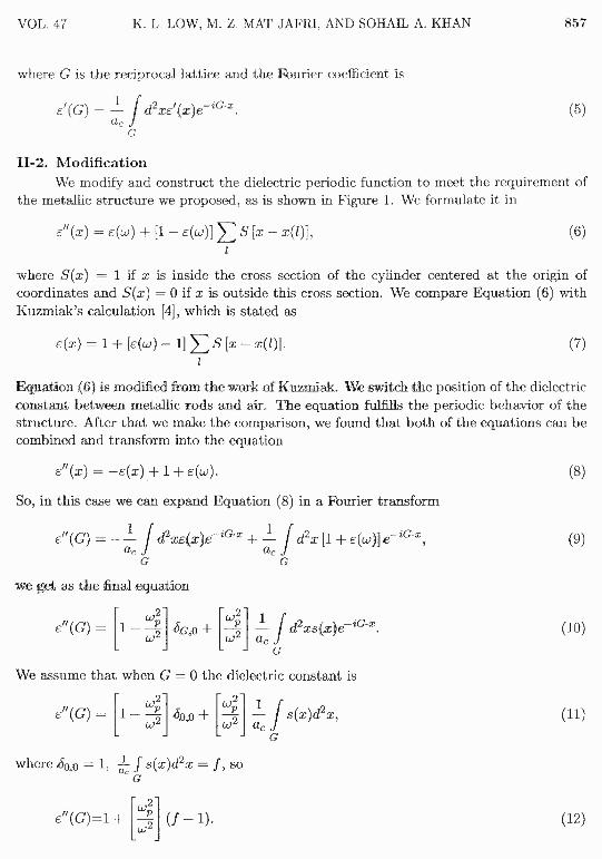
VOL. 47 K. L. LOW, M. Z. MAT JAFRI, AND SOHAIL A. KHAN 857
where G is the reciprocal lattice and the Fourier coefficient is
(G — f d2X£1(X)CIG.xa, (5)
11-2. ModificationWe modify and construct the dielectric periodic function to meet the requirement of
the metallic structure we proposed, as is shown in Figure 1. We formulate it in
s"(x) = e(w) + [1 — E(w)]
S [x — x(1)], (6)
where S(x) = 1 if x is inside the cross section of the cylinder centered at the origin ofcoordinates and S(x) = 0 if x is outside this cross section. We compare Equation (6) withKuzmiak's calculation [4], which is stated as
e(x) = 1 + [e(w) —
S [x — x(1)]. (7)
Equation (6) is modified from the work of Knzmiak We switch the position of the dielectricconstant between metallic rods and air. The equation fulfills the periodic behavior of thestructure. After that we make the comparison, we found that both of the equations can becombined and transform into the equation
E" (X) = —e(x) + 1 + E(w). (8)
So, in this case we
1
can expand Equation (8) in a Fourier transform
Ell (G) _ _ 1___ f d2 xE(x)e—iG-x + _ f d2 x [1 + E (0] e—iG-x,a, a,
G G
we get as the final equation
1— —coP2
(5040+ —P2 —ac d2.xs(z)e—iG-x . (10)[,.,2
Ell(G)=
]1
w2
Gw
We assume that when G = 0 the dielectric constant is
]w2 60
CO2
1E" (G) = [ 1 — -3), i) + --iw —a f s(x)d2x,
C G
where 40,0 = 1, -a71 f s(x)d2x = f, so
Lo2
e"(G)-=1 +Lil
— 1).
(9)
(12)

858 BAND GAP CALCULATION USING ... VOL. 47
We also assume that when G 0 the dielectric constant is
Eft (G) = [1 e-,1 A [ d.sxs(x)e—iG-sW2 •-n` a,
2 2W„, W, 1
where 5G,0 = 0, IGIR soas1 f s(x)e- iG - x d2x = 2./J1(IGIR)
E" (G) = 2f [ w2P] (IG,IR) ,„2 pvi •
11-3. ApplicationAfter the calculation of the dielectric, which is most important for finding the band
gap, we will apply Maxwell's equations. In this application, we would like to consider onlythe E polarization mode or transverse magnetic mode.
In the TM mode (E polarization) E3 (xNW) is obtained as
E3(x i c'-') =
B(k1G)é(k±c)"2, (15)
where k is the wave vector of the wave. Then, we obtained an equation (16) satisfied bythe coefficients B(kIG):
(k + G) 2 B(kiG) =C
e(G - G')B(kIG)
-2
E(0)B(kIG) + — (G - G')B(k(G). (16)c2
The use of the results of Equations (12) and (14) into Equation (16) which transforms thelatter into
„02 0)2 9 elt CiR)B(kiG)(k + G) 2 B(kIG) - f-- 1 B(kIG) + B(kIG)-c2G
_
= 2- B(kIG)c2
[W2tog <11 (IG — IR) x B(kIG)P 2f(k + G)26G,G, ± ---0G4G' c2IG - GIIIR
= ::-B(kIG). (17)c2
III. RESULTS AND DISCUSSION
Equation (17) is a Hermitian Matrix. It has eigenvalues that need to be found. Thisis a standard eigenvalue problem that can numerically be solved. We used copper as the

TWIlBand swtWn of a2029 S quan:Dhaanic ,band slructure
2
12
IA
0:2
0
VOL. 47 K. L. LOW, M. Z. MAT JAFRI, AND SOHAIL A. KHAN 859
metal slab and a vacuum for the cylinder rods. The plasma frequency of copper is 1914TIiz110]. We applied this equation into 2 different lattice arrangements. First, we will usethe square lattice arrangement and then the triangular lattice arrangement.
1. Square lattice
We first consider a simple square lattice arrangement. The lattice parameter is a for whichthe primitive translation vectors are
al = a(1, 0), a2 = a(0, 1), (18)
while the vectors of the reciprocal lattice are
27r , 2rb i = b2 — (19)
a a
The filling fractions of the square lattice air rods in the metallic slab are f 71R2/a2.
a)
c)
FIG. 2: (a) Square lattice arrangement. (b) Band structure of 2D square lattice with filling factor=0.0001, a = 1 mm, and R= (011056 11011,, (e)) filling factor= a.3,, a = 1 mm, and R = 0.3090 mm
The arrangement of the square lattice is shown in Figure 2(a). The photonic band gapis presented in Figure 2(b) and 2(c) with different filling fractions. We used a total of 121
860 BAND GAP CALCULATION USING ... VOL. 47
0.45
035
03
025
02
0.15
0.05
0 0.05 .0.1 0_15 02 0.25 03 0.35 DA
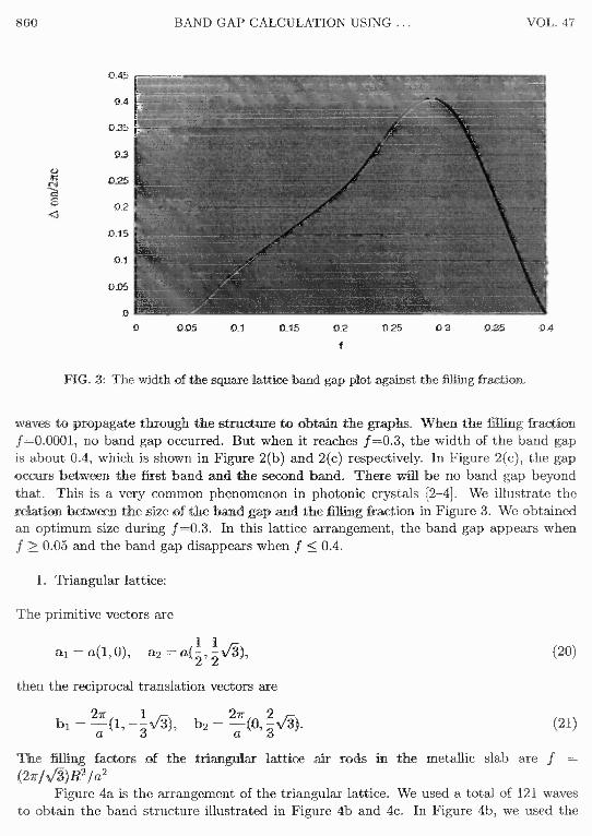
FIG. 3: The width of the square lattice band gap plot against the filling fraction.
waves to propagate through the structure to obtain the graphs. When the filling fractionf=0.0001, no band gap occurred. But when it reaches f=0.3, the width of the band gapis about 0.4, which is shown in Figure 2(b) and 2(c) respectively. In Figure 2(c), the gapoccurs between the first band and the second band. There will be no band gap beyondthat. This is a very common phenomenon in photonic crystals [2-4]. We illustrate therelation between the size of the band gap and the filling fraction in Figure 3. We obtainedan optimum size during f=0.3. In this lattice arrangement, the band gap appears whenf > 0.05 and the band gap disappears when f < 0.4.
1. Triangular lattice:
The primitive vectors are
1 ' "1 t7,-,
'a l = a(1, 0),
a2 a(-2(20)
then the reciprocal translation vectors are
b1 b2 21 30 1. (21)a I
The filling factors of the triangular lattice air rods in the metallic slab are f(27r/AR2/a2
Figure 4a is the arrangement of the triangular lattice. We used a total of 121 wavesto obtain the band structure illustrated in Figure 4b and 4c. In Figure 4b, we used the

VOL. 47 K. L. LOW, M. Z. MAT JAFRI, AND SOHAIL A. KHAN 861
FIG. 4: a) Triangular lattice arrangement_ b) Band structure of 2D triangle lattice with fillingfactor= 0.0001, a = 1 mm, R 0.0053 ram; c) filling factor= 0_3, a = 1 mm and R = 0.2876 mm
itliddand barubzurnmda2Dtiansularbbnbonic band strundurs TM:Band stnatase of a 2D inanglnar phatonrc band st manta
a)
b)
FIG. 5: a) Band structure of a 2D triangle lattice with filling factor= 0.4, a = 1 mm, R = 0.3321ram; b.) filling factor= 0_5, a = 1 mm, and R = 0.3713 mm

862 BAND GAP CALCULATION USING ... VOL. 47
filling fraction f=0_0001. No band gap appears in this filling fraction_ In Figure 4c, we usef=0.3 and a band gap appears in this structure. As usual, the gap only appears in betweenthe first band and second band. The band structure shows that the band gap appears inbetween the third band and fourth band for Figure 5a, while there is a second band andthird band for Figure 5b. Figure 5a shows the band structure of the photonic crystals withf =0.4 and Figure 5b for f =0.5. This phenomenon is very rare.
0A
0.35
03
025
02
0.15
01
0.05
0 0
0.1
02
0.3
0.4
0.5
0.6
0.7
FIG. 6: The width of the square lattice band gap plot against the filling fraction.
We plot the relation between the gap size and the filling fraction. This is illustratedin Figure 6. We find that there are 2 peaks, although another one is smaller when f =0.5.
In this lattice arrangement, the gap appears when f > 0 and only disappears when f < 0.6.Although the gap size is getting smaller when f a 0.4, it rises again after that. The energywill be emitted again after a peak. So, this condition can be used when the band energywhich is needed is not from the first band.
IV. CONCLUSIONS
The wave expansion method has been successfully used to calculate the band gapstructure of a metallic slab with air rods. We only used 121 waves to obtain a very accurateresult. From this investigation, we find that the band energy, no matter what filling fraction,does not tend to zero at F. A 2D square lattice band gap appears in between the first and

VOL. 47 K. L. LOW, M. Z. MAT JAFRI, AND SOHAIL A. KHAN 863
second band for all of the filling fractions. However, for the 2D triangular lattice, the bandgap appears in between the second band and the third band, as well as the third and fourthband for f =0.4 and f= 0.5, respectively. Although the size of the gap is small, it still canbe applied if the needed transmittal energy starts from the second band or third band. So,it can be used in different applications of metallic slabs. Our method of calculation can beextended to find the band gap structure of defect modes and waveguide modes of photoniccrystals which are made of metallic slabs.
Acknowledgements
This project was carried out using the Fundamental Research Grants Scheme (FRGS)with grants number 203/PFIZIK/671166. We would like to thank the technical staff whoparticipated in this project. Thanks are extended to USM for support and encouragement.
References
[1] E. Yablonovitch, J. Opt. Soc. Am. B 10, 13 (1993).(2] D. Hermann, M Frank, K Busch, and P Woliie, Opt. Express 8 (2001).
M. Plihal and A. A. Maradudin, Phys. Rev. B 44, 7 (1991).V. Kuzmiak, A. A. Maradudin, and F. Pincenmin, Phys. Rev. B 50, 10 (1994).Y.-S. Zhou, B.-Y. Gu, and F.-H. Wang, Euro. Phys. J. B 37, 7 (2004).S. K. Parui and S. Das, in First India Annual Conference, 2004. Proceedings of the IEEEINDICON 2004 (IEEE, 2004).S. Guo and S. Albin, Opt Express 11, 9 (2003).K. Rambabu, M. Mokhtaari, and J. Borneman, in Electromagnetic Compatibility, IEEE Inter-national Symposium on EMC 2007, 2007).
(9] 1 J. Simpson, A. Tallow, 1 A. Mix, and H. Heck, IEEE Transactions on Microwave Theoryand Techniques 54 (2006).
[10] El-Kady, M. M. Sigalas, R. Biswas, K. M. Ho, and C. M. Soukoulis, Phys. Rev. B 62, 4 (2000).


![PEPERIKSAAN PERCUBAAN SIJIL PELAJARAN MALAYSIA 2018 … Physics P2 Johor… · selari perpendicular serenjang [1 mark/ 1 markah] Radiowave Gelombang radio Microwave Gelombang mikro](https://static.fdokumen.site/doc/165x107/609a6bff1aee82188d618613/peperiksaan-percubaan-sijil-pelajaran-malaysia-2018-physics-p2-johor-selari-perpendicular.jpg)