PERPUSTAKAAN UTHM - COnnecting REpositories · menunjukkan yang walaupun nilai Ie adalah lebih...
24
Transcript of PERPUSTAKAAN UTHM - COnnecting REpositories · menunjukkan yang walaupun nilai Ie adalah lebih...

PERPUSTAKAAN UTHM
\\\\!\I\\~\\~\\~\\~\~\\\\\I\\\I\I\\~\\\\\\\\\\\~\\\\\ Oi!l •.• " *30000002343755*
UNIVERSITI TUN HUSSEIN ONN MALAYSIA
STATUS CONFIRMATION FOR MASTER'S PROJECT REPORT
AN EVALUATION ON THE CONTRIBUTION OF DIFFERENTIAL MODE
AND COMMON MODE CURRENTS IN RADIATED EMISSION OF
DIGITAL CIRCUITS
ACADEMIC SESSION: 2008/2009
I, AIZA MAHYUNI BINTI MOZI, agree to allow this Master's Project Report to be kept at the Library under the following terms:
I. This Master's Project Report is the property of the Universiti Tun Hussein Onn Malaysia. 2. The library has the right to make copies for educational purposes only. 3. The library is allowed to make copies of this report for educational exchange between higher
educational institutions. 4. ** Please mark C")
II II CONFIDENTIAL
II II RESTRICTED
II" II FREE ACCESS
(WRITER' lliNA TURE)
Permanent address:
6 JALAN PERMAI, TAMAN INDAH, 83710 PARIT YAANI, YONG PENG, JOHOR.
Date: MAY 2009
NOTE:
(Contains information of high security or of great importance to Malaysia as STIPULATED under the OFFICIAL SECRET ACT 1972)
(Contains restricted information as determined by the organization/institution where research was constructed)
Approved by,
AtJ~
PROF. DR. MOHD. ZARAR BIN MOHD.JENU
Date: MAY 2009
** If this Master's Project Report is classified as CONFIDENTIAL or RESTRICTED, please attach the letter from the relevant authority/organization stating reasons and duration for such classifications.
AN EVALUATION ON THE CONTRIBUTION OF DIFFERENTIAL MODE
AND COMMON MODE CURRENTS IN RADIATED EMISSION OF
DIGITAL CIRCUITS
AIZA MAHYUNI BINTI MOZI
A project report submitted in partial
fulfilment of the requirement for the award of the
Degree of Master of Electrical Engineering
Faculty of Electrical and Electronic Engineering
Universiti Tun Hussein Onn Malaysia
MAY 2009
I hereby declare that the work in this project report is my own except for quotations
and summaries which have been duly acknowledged .
Student
Date
Supervisor
Date
..... ~~.: ...................... .
AIZA MAHYUNI BINT! MOZI
MAY 2009
1i/~ ........... r ............. ~ ...... . PROF. DR. MOHD. ZARAR BIN MOHD. JENU
MAY 2009
ii

iii
For my beloved parents andJamily.
iv
ACKNOWLEDGEMENT
Alhamdulillah, first and foremost I would like to thank God, for giving me the
opportunity to complete my Master's Project entitle An Evaluation on the
Contribution of Differential Mode and Common Mode Currents in Radiated
Emission of Digital Circuits.
My highest gratitude to Prof. Dr. Mohd. Zarar Bin Mohd. Jenu as the Project
Supervisor for the supervision and unfailing patience throughout my Master's
Project. Without his guidance and invaluable time spent with me in this experimental
study, this Master's Project would not have been completed successfully.
Not also forgotten, EMC Center staffs Mr. Mohd. Erdi Bin Ayob, Mr
Saizalmursidi bin Md. Mustam, and Mr. Mohd. Nazeri Bin Sarmijan for the helps
and useful advices in completing my laboratory and experimental work. Other than
that, I also would like to thank alI my friends for their cooperation and assistances.
Last but not least, I would like to thank my family for their endless love and
faith on me to complete this Master's Project. May God bless you.
Thank you.
v
ABSTRACT
Electromagnetic Compatibility (EMC) is an issue that has rapidly increased in
importance in recent years, driven by legal, and conunercial demands. The EMC
compliance requires the implementation of a total EMC approach to the development
of electric and electronic circuitry such as in product manufacturing, with
compliance being an integral part of the product life-cycle. Radiated emission test is
one of the EMC criteria with a purpose to ensure that other products are protected
from the emissions generated by it. TIns project is focused on the contribution of
Differential Mode Current (Id) and Conunon Mode Current (Ie), that occur in electric
and electronic circuitry wmch definitely affects the overall radiated emissions level.
A standard test circuit was designed and implemented as the reference circuit.
Several of the test circuits were designed and developed using appropriate layout
design techniques such as loop area control and appropriate grounding techniques to
ensure signal quality and functional performances due to EMC. The value of Id
exhibited significantly much mgher values than Ie for frequency ranges between 30
MHz to 1000 MHz throughout all the measurements. Despite the significantly
different values between Id and Ie , the total radiated emissions over the frequency
ranges exlnbited consistent results. Tms indicate that although the values of Ie were
noticeably lower than Id, Ie still dominated the radiated emission in electric and
electronic circuitry. The effects of loop area and grounding techniques on radiated
emission were also studied. There was a 0.3 % of reduction regarding loop area
technique using double-sided PCB compared to the standard test circuit. The average
value of radiated emission produced by the test circuit due to Id exhibited a reduction
of3.42 % from the standard test circuit, wmle the average value of radiated emission
produced by the test circuit due to Ie exhibited a reduction of 2.17 % from the
standard test circuit. Future work should focus on improving the circuit design and
development using multilayer PCB for optimal performance. Furthermore, effort can

also be made on expanding the circuit design by implementing noisy sources such
relays and motors, and improve the circuit with higher density and more traces.
vi
vii
ABSTRAK
Keserasian elektromagnet (EMC) adalah satu isu penting yang meningkat dengan
begitu cepat pada kebelakangan tahun ini, yang disebabkan oleh permintaan terhadap
undang-undang dan permintaan komersial. Kepatuhan terhadap keserasian
elektromagnet memerlukan pendekatan perlaksanaan keserasian elektromagnet
sepenulmya ke atas proses pembangunan sesebuah litar elektrik dan eleh.1:ronik
seperti di dalarn penghasilan produk di mana kepatuhan terhadap keserasian
elektromagnet adalah salah satu kitaran hidup produk tersebut. Ujian terhadap sinar
pancaran merupakan salah satu kriteria di dalarn keserasian elektromagnet, di mana
ia khususnya bertujuan memastikan sesuatu produk dilindungi dari pancaran sinar
yang terhasil. Projek ini memfokus terhadap sumbangan mod berbeza arus aliran
elektrik (Id) dan mod biasa arus aliran elektrik (Ie), yang wujud di dalarn sesebuah
litar elektrik dan elektronik, yang mana ia semestinya memberi kesan terhadap paras
sinar pancaran yang terhasil. Sebuah litar ujian piawai telah direkabentuk dan
diaplikasikan sebagai litar rujukan. Beberapa litar ujian telah direkabentuk dan
dihasilkan menggunakan teknik-teknik rekaan yang baik seperti teknik mengawal
keluasan litar dan teknik pemburnian bagi memastikan penghasilan isyarat yang
berkualiti dan bermutu terhadap keserasian elektromagnet. Di dalarn setiap ujikaji,
nilai Id memparnerkan bacaan yang sangat tinggi berbanding nilai Ie bagi julat
frekuensi di antara 30 MHz ke 1000 MHz. Akan tetapi, di sebalik terdapatnya
perbezaan nilai yang besar antara Id dan Ie, sinar pancaran yang terhasil
menunjukkan bacaan keputusan yang konsisten antara satu sarna lain. Jni
menunjukkan yang walaupun nilai Ie adalah lebih rendall berbanding nilai Id, Ie
tetap mendominasi sinar pancaran yang terhasil dari litar elektrik dan elektronik.
Kesan terhadap keluasan litar dan teknik pembumian juga telah dikaji. Terdapat
pengurangan sebanyak 0.3% terhadap teknik keluasan kawasan yang digunakan pada
PCB dua-belah berbanding litar ujian piawai. Nilai purata sinar pancaran yang
terhasil oleh litar ujian yang disebabkan oleh Id, menunjukkan pengurangan

viii
sebanyak 3.42 % berbanding litar ujian piawai, manakala purata sinar pancaran yang
terhasil oleh litar ujian yang disebabkan oleh Ie, menunjukkan pcngurangan
sebanyak 2.17 % berbanding litar ujian piawai. Kajian lanjutan scharusnya
memfokus kepada penambahbaikkan rekabentuk dan pcmbinaan litar menggunakan
PCB berbilang lapisan untuk perlaksanaan yang optimum. Focus juga bolch
dilakukan ke atas mengembangkan rekabentuk litar dengan menggunakan sumbcr
yang mempunyai nilai hingar yang tinggi seperti motor, dan menambahbaik litar
dengan kepadatan yang lebih tinggi dan laluan yang lebih banyak.
TABLE OF CONTENTS
MASTER'S PROJECT STATUS CONFIRMATION
TITLE
DECLARATION
DEDICATION
ACKNOWLEDGEMENT
ABSTRACT
ABSTRAK
TABLE OF CONTENTS
LIST OF FIGURES
LIST OF SYMBOLS AND ABREVIATIONS
CHAPTER 1 INTRODUCTION
1.1 General
1.2 Problem Statement
1.3 Aim of Study
1.4 Objectives
1.5 Significance of Study
1.6 Outline of the Report
CHAPTER 2 LITERATURE REVIEW
2.1 Introduction
2.2 PCB Basics
2.2.1 EMC and the PCB
ii
III
iv
v
vii
IX
xiii
PAGE
3
5
5
6
6
8
8
10
ix
x
2.2.2 RF Energy Developed Within PCB 11
2.3 Grounding 14
2.3.1 Fundamental Grounding Concepts 14
2.3.2 Ground Plane on PCB 16
2.4 Radiated Emission 16
2.4.1 Differential Mode versus Common Mode Current 18
2.4.2 Differential Mode Current Emission Model 19
2.4.3 Common Mode Current Emission Model 20
2.5 Review of Research Works on EM Emission 21
CHAPTER 3 RESEARCH METHODOLOGY
3.1 Introduction 23
3.2 Review of Experiment Procedures 23
3.3 Review of Standard Test Circuit 26
3.3.1 Design and Develop Standard Test Circuit 28
3.3.2 Characteristic Impedance Measurement 29
3.3.3 Voltage Measurement 30
3.4 Design and Develop Test Circuit
Using Single-Sided PCB 33
3.4.1 Design and Develop Test Circuit 1 33
3.4.2 Design and Develop Test Circuit 2 34
3.4.3 Design and Develop Test Circuit 3 35
3.5 Design and Develop Test Circuit
Using Double-Sided PCB 36
3.5.1 Design and Develop Test Circuit 4 37
3.5.2 Design and Develop Test Circuit 5 37
3.5.3 Design and Develop Test Circuit 6 39
3.6 Design and Develop Test Circuit
for EMC Compliance / Enhancement 40
3.6.1 Design and Develop Test Circuit 7 40
3.6.2 Design and Develop Test Circuit 8 41
3.7 Emission due to Differential Mode Current 42
3.8
3.9
Emission due to Common Mode Current
Experimental Measurement
CHAPTER 4 RESULTS AND DISCUSSIONS
4.1 Introduction
4.2 Standard Test Circuit
4.2.1 Evaluation on Standard Test Circuit
4.3 Test Circuit Using Single-Sided PCB
4.3.1 Test Circuit 1
4.3.1.1 Evaluation on Test Circuit 1
4.3.2 Test Circuit 2
4.3.2.1 Evaluation on Test Circuit 2
4.3.3 Test Circuit 3
4.3.3.1 Evaluation on Test Circuit 3
4.3.4 Summary
4.4 Test Circuit Using Double-Sided PCB
4.4.1 Test Circuit 4
4.4.1.1 Evaluation on Test Circuit 4
4.4.2 Test Circuit 5
4.4.2.1 Evaluation on Test Circuit 5
4.4.3 Test Circuit 6
4.4.3.1 Evaluation on Test Circuit 6
4.4.4 Summary
4.5 Test Circuit for EMC Compliance
4.5.1 Test Circuit 7
4.5.1.1 Evaluation on Test Circuit 7
4.5.2 Test Circuit 8
4.5.2.1 Evaluation on Test Circuit 8
4.5.3 Summary
4.6 Summary
43
44
49
49
50
52
52
53
55
56
57
57
60
61
61
63
64
65
67
69
71
74
74
75
77
78
80
83
xi
CHAPTER 5 CONCLUSION AND FUTURE PLANNING
5.1
5.2
5.2
Introduction
Conclusion
Future Planning
REFERENCES
APPENDICES
87
87
89
91
94
xii
xiii
LIST OF FIGURES
FIGURE TITLE PAGE
1.1 The field ofEMC 2
1.2 Radiated emission from an interface cable is usually called differential mode radiation 3
1.3 Radiated emission from on well-defined circuit loop is usually called common mode radiation 3
1.4 Graph of incorporating EMC measures throughout product development cycle 5
2.1 The cross-sectional dimensions of lines composed of rectangular cross-section conductor for a PCB consisting of strips on the same side 9
2.2 The cross-sectional dimensions of lines composed of rectangular cross-section conductor for a PCB consisting of strips on the opposite side 10
2.3 Component characteristic at RF frequencies I I
2.4 Radiated emission emits from a computer 17
2.5 The mechanism of radiated emission 18
2.6 The composition of total currents into Ie and Id components 19
2.7 A simplified estimate of the maximum radiated emission due to Id 20
2.8 A simplified estimate of the maximum radiated emission due to Ie 21
3.1 The project methodology flow 25
3.2 The schematic of test circuit within a single-sided PCB 27
3.3 TIle measurcd and predicted radiated emission 27
3.4 A test circuit has been designed and implemented as the standard test circuit. 28
3.5 Oscillator output of I OMHz trapezoidal pulse train 28
xiv
3.6 A finite length of line is terminated in its characteristic impedance, Zo, therefore, its input impedance will also equal Zo 29
3.7 Characteristic Impedance measurement using MA TLAB 30
3.8 Command Window result from MA TLAB 30
3.9 The illustration of Faraday's law towards the probe meter 31
3.10 Probe meter 32
3.11 The top side and bottom side of test circuit 1 34
3.12 The top side and bottom side of test circuit 2 35
3.13 The top side and bottom side of test circuit 3 36
3.14 The top side and bottom side of test circuit 4 38
3.15 The top side and bottom side of test circuit 5 38
3.16 The top side and bottom side oftest circuit 6 39
3.17 The upper side and bottom side of test circuit 7 41
3.18 The upper side and bottom side of test circuit 8 42
3.19 The Id and Ie currents decomposition in a matched load closed loop test circuit. 43
3.20 The Ie currents decomposition in an opened loop test circuit 44
3.21 The actual GTEM cell used for evaluating radiated emission within this experimental study 45
3.22 The diagram of emission measurements test set up of a GTEM 750 cell 46
3.23 The three positions selection ofEUT in GTEM cell 46
3.24 The position of test circuit in y-axis 47
3.25 The position of test circuit in z-axis 47
3.26 The position of test circuit in x-axis 48
4.1 Emission (measured) and Id (calculated) for the standard test circuit 50
4.2 Emission (measured) and Ie (calculated) for the standard test circuit 50
4.3 Emission (measured) and Id (calculated) for test circuit 1 52
4.4 Emission (measured) and Ie (calculated) for test circuit 1 53
4.5 Emission (measured) and Id(calculated) for test circuit 2 55
4.6 Emission (measured) and Ie (calculated) for test circuit 2 55
4.7 Emission (measured) and Id (calculated) for test circuit 3 58
4.8 Emission (measured) and Ie (calculated) for test circuit 3 58
4.9 Emission (measured) and Id (calculated) for test circuit 4 62
xv
4.10 Emission (measured) and Ie (calculated) for test circuit 4 62
4.11 Emission (measured) and Id (calculated) for test circuit 5 65
4.12 Emission (measured) and Ie (calculated) for test circuit 5 65
4.13 Emission (measured) and Id(calculated) for test circuit 6 (Load terminated at point 1) 68
4.14 Emission (measured) and Id (calculated) for test circuit 6. (Load terminated at point 2). 68
4.15 Emission (measured) and Ie (calculated) for test circuit 6 69
4.16 Emission (measured) and Id (calculated) for test circuit 7 74
4.17 Emission (measured) and Ie (calculated) for test circuit 7 75
4.18 Emission (measured) and Id (calculated) for test circuit 8 77
4.19 Emission (measured) and Ie (calculated) for test circuit 8 78
B
E
f I
jX
R
s
v 11'
Z
E,max
Ee.max
Ie
Id
ITt
Vprobe
VTt
Zc
Zo
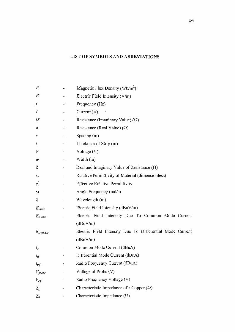
LIST OF SYMBOLS AND ABREVIATIONS
Magnetic Flux Density (Wb/m2)
Electric Field Intensity (V 1m)
Frequency (Hz)
Current (A)
Resistance (Imaginary Value) (.0.)
Resistance (Real Value) (.0.)
Spacing (m)
Thickness of Strip (m)
Voltage (V)
Width (m)
Real and Imaginary Value of Resistance (.0.)
Relative Permittivity of Material (dimensionless)
Effective Relative Permittivity
Angle Frequency (radls)
Wavelength (m)
Electric Field Intensity (dBuV/m)
xvi
Electric Field Intensity Due To Common Mode Current
(dBuV/m)
Electric Field Intensity Due To Differential Mode Current
(dBuV/m)
Common Mode Current (dBuA)
Differential Mode Current (dBuA)
Radio Frequency Current (dBuA)
Voltage of Probe (V)
Radio Frequency Voltage (V)
Characteristic Impedance of a Copper (.0.)
Characteristic Impedance (.0.)

EMC
EUT
emf
FCC
GTEM
PCB
RF
Electromagnetic Compatibility
Equipment Under Test
Electromotive Force
Federal Communications Commission
Gigahertz Transverse Electromagnetic Mode
Printed Circuit Board
Radio Frequency
xvii
CHAPTER 1
INTRODUCTION
1.1 General
In many countries, the necessities to meet up with the EMC requirements of digital
devices are in great demand. The continued market growth in portable electrics and
electronics, advanced control systems for transportation and computerized factories
have flooded the Radio Frequency (RF) spectrum. The increases in RF noise make
EMC of digital devices essential in insuring continued expected operation.
Generally, EMC indicates the capability of electrical and electronic system,
equipment and devices to operate in its intended electromagnetic environment within
a defined margin of safety, and at design levels or performance, without suffering or
causing unacceptable degradation as a result of electromagnetic interference [1]. A
system is electromagnetically compatible with its environment if it satisfies these
three criterions; it does not cause interference with other systems, it is not susceptible
to emissions from other systems and it does not cause interference with itself [2].
The field ofEMC consists of two distinct areas which are emissions and
susceptibility as shown in Figure 1.1. Emissions are the propagation of
electromagnetic interference from noncompliant devices (culprits), in particular,
radiated and conducted electromagnetic interference. On the other hand,
susceptibility is the detrimental effects on susceptible devices (victims) in the form
that include radiated and conducted electromagnetic interference. Consequently,
EMC subproblems comprise of radiated emission, conducted emission, radiated
susceptibility and conducted susceptibility. However, this experimental study will
only focus on one of those subproblems which are radiated emission. On the whole,
1
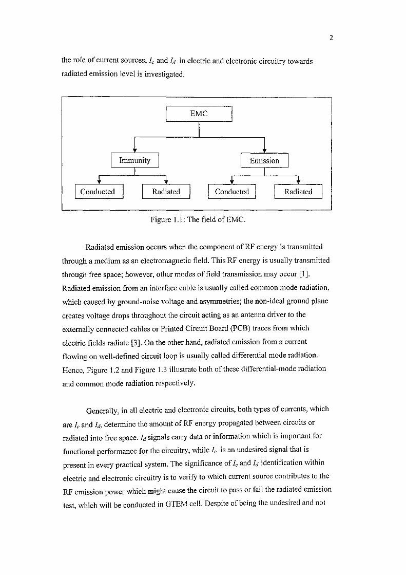
the role of current sources, Ie and Id in electric and electronic circuitry towards
radiated emission level is investigated.
Figure 1.1: The field of EMC.
Radiated emission occurs when the component of RF energy is transmitted
through a medium as an electromagnetic field. This RF energy is usually transmitted
through free space; however, other modes offield transmission may occur [1].
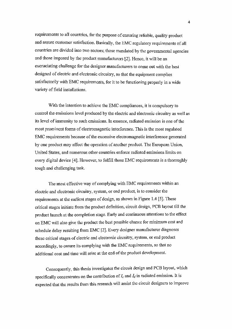
Radiated emission from an interface cable is usually called common mode radiation,
which caused by ground-noise voltage and asymmetries; the non-ideal ground plane
creates voltage drops throughout the circuit acting as an antenna driver to the
externally connected cables or Printed Circuit Board (PCB) traces from which
electric fields radiate [3]. On the other hand, radiated emission from a current
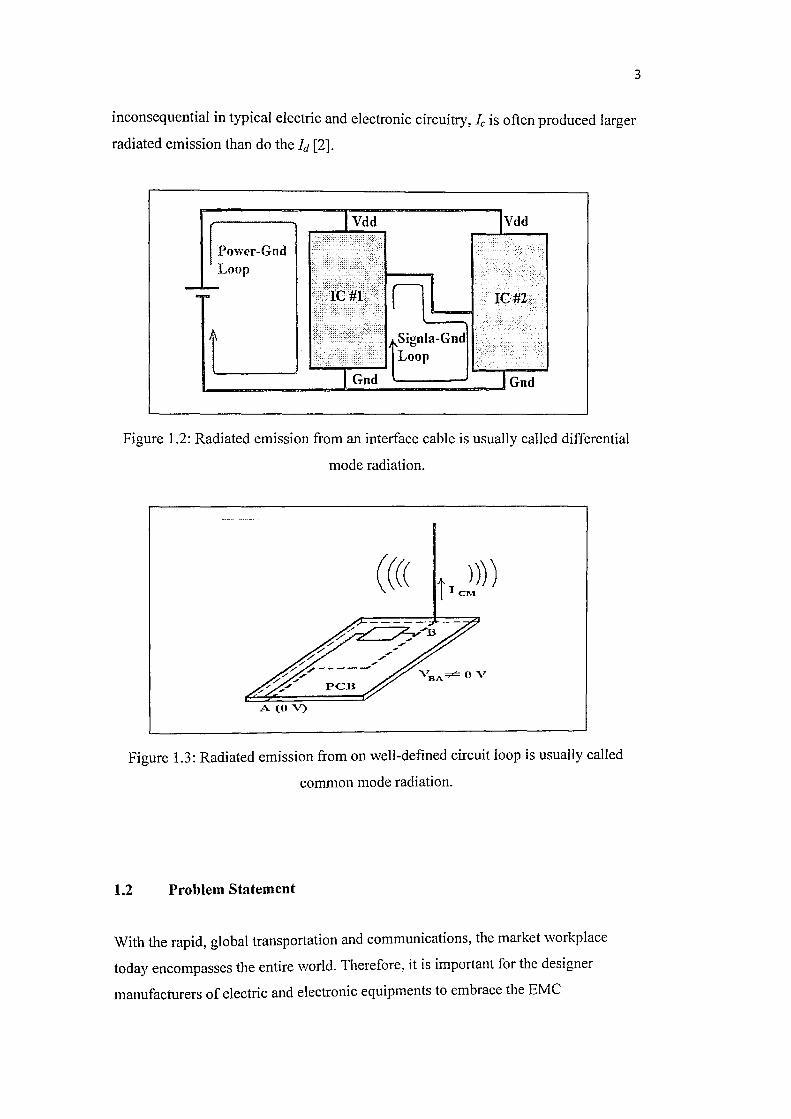
flowing on well-defined circuit loop is usually called differential mode radiation.
Hence, Figurc 1.2 and Figure 1.3 illustrate both of these differential-mode radiation
and common mode radiation respectively.
2
Generally, in all electric and electronic circuits, both types of currents, which
are Ie and Id, determine the amount of RF energy propagated between circuits or
radiated into free space. Id signals carry data or information which is important for
functional performance for the circuitry, while Ie is an undesired signal that is
present in every practical system. The significance of Ie and Id identification within
electric and electronic circuitry is to verify to which current source contributes to the
RF emission power which might cause the circuit to pass or fail the radiated emission
test, which will be conducted in GTEM cell. Despite of being the undesired and not
3
inconsequential in typical electric and electronic circuitry, Ie is often produced larger
radiated emission than do the Id [2].
PO'r .... ('r-Gnd Loop
Figure 1.2: Radiated emission from an interface cable is usually called differential
mode radiation.
((((
A (0 V)
Figure 1.3: Radiated emission from on well-defined circuit loop is usually called
common mode radiation.
1.2 Problem Statement
With the rapid, global transportation and communications, the market workplace
today encompasses the entire world. Therefore, it is important for the designer
manufacturers of electric and electronic equipments to embrace the EMC
4
requirements to all countries, for the purpose of ensuring reliable, quality product
and assure customer satisfaction. Basically, the EMC regulatory requirements of all
countries are divided into two sectors; those mandated by the governmental agencies
and those imposed by the product manufacturers [2]. Hence, it will be an
excruciating challenge for the designer manufacturers to come out with the best
designed of electric and electronic circuitry, so that the equipment complies
satisfactorily with EMC requirements, for it to be functioning properly in a wide
variety of field installations.
With the intention to achieve the EMC compliances, it is compulsory to
control the emissions level produced by the electric and electronic circuitry as well as
its level of immunity to such emissions. In essence, radiated emission is one of the
most prominent forms of electromagnetic interference. This is the most regulated
EMC requirements because of the excessive electromagnetic interference generated
by one product may affect the operation of another product. The European Union,
United States, and numerous other countries enforce radiated emissions limits on
every digital device [4]. However, to fulfill those EMC requirements is a thoroughly
tough and challenging task.
The most effective way of complying with EMC requirements within an
electric and electronic circuitry, system, or end product, is to consider the
requirements at the earliest stages of design, as shown in Figure 1.4 [5]. These
critical stages initiate from the product definition, circuit design, PCB layout till the
product launch at the completion stage. Early and continuous attentions to the effect
on EMC will also give the product the best possible chance for minimum cost and
schedule delay resulting from EMC [2]. Every designer manufacturer diagnoses
these critical stages of electric and electronic circuitry, system, or end product
accordingly, to ensure its complying with the EMC requirements, so that no
additional cost and time will arise at the end of the product development.
Consequently, this thesis investigates the circuit design and PCB layout, which
specifically concentrates on the contribution of Ie and Id in radiated emission. It is
expected that the results from this research will assist the circuit designers to improve