UNIVERSITI TEKNOLOGI MALAYSIA -...
21
OPTICAL AND SENSING PROPERTIES OF SPUTTERED INDIUM TIN OXIDE (ITO) THIN FILMS MOHAMAD HELMI BIN ABD MUBIN UNIVERSITI TEKNOLOGI MALAYSIA
Transcript of UNIVERSITI TEKNOLOGI MALAYSIA -...
OPTICAL AND SENSING PROPERTIES OF SPUTTERED INDIUM TIN
OXIDE (ITO) THIN FILMS
MOHAMAD HELMI BIN ABD MUBIN
UNIVERSITI TEKNOLOGI MALAYSIA
OPTICAL AND SENSING PROPERTIES OF SPUTTERED INDIUM TIN OXIDE
(ITO) THIN FILMS
MOHAMAD HELMI BIN ABD MUBIN
A thesis submitted in fulfilment of the
requirements for the award of the degree of
Master of Science (Physics)
Faculty of Science
Universiti Teknologi Malaysia
JANUARY 2014
iii
Dedicated to my beloved parents,
Abd Mubin Bin Othman and Kalsom Begum Binti Fazal Ahmad,
to my siblings and family,
to my fiance, Nur Fatin Binti Sulaiman,
to my friends,
thank you so much,
for their patience, support, love and encouragement.
iv
ACKNOWLEDGEMENT
In the name of Allah s.w.t, the most gracious and the most merciful
Firstly, I wish to express my sincere appreciation to my supervisor, Dr. Wan
Nurulhuda Wan Shamsuri and my co-supervisor, Dr. Khamim Bin Ismail for giving
me an opportunity for this research. I am also grateful for the support, guidance,
patient and imparting their knowledge for me. Writing this thesis is a remarkable
accomplishment, thanks for their advices.
Furthermore, I would also like to thank all lecturers and laboratory assistants
from the Department of Physics for their help and advice during this research. I am
also grateful to my supervisor and Universiti Teknologi Malaysia for the financial
support through the GUP vote.
Besides that, I would like to show my appreciation to my research team and
my friends for their supports, ideas and information for me to complete this research.
Lastly, I would like to express my gratitude to my beloved family members, my
father, Abd Mubin Bin Othman, my mother, Kalsom Begum Binti Fazal Ahmad, my
younger brother, Abdul Hadi and my fiance, Nur Fatin Binti Sulaiman. Thanks for
all the love, support and encouragement.
v
ABSTRACT
Two sets of indium tin oxide thin film were prepared at different thicknesses onto the
corning glass substrates using radio frequency magnetron sputtering method. Set one
is for single configuration sample and set two is for sensor array sample. All
samples were annealed at temperature of 600°C for 4 hours inside a furnace. A
surface profiler was used to measure the thickness of the samples while a UV-VIS
spectrophotometer was used to measure their optical properties. The gas sensing
characterization system was used to determine the gas sensing properties in 200 ppm
of nitrogen dioxide, NO2. The thickness of the sample was found to be in the range
of 132 nm to 424 nm. The transmittance and the optical band gap decrease as
thickness increases. The resistance decreased to several kilo ohms when the
operating temperature increased for all samples. The highest sensitivity for single
configuration was found in sample C with thickness 227 nm (45 minutes deposition
time). Sample H has the highest sensitivity (combination of 15 minutes + 90 minutes
deposition times) for array configuration. Thus, the response time and the
corresponding recovery time for sample C were 66.6 seconds and 133.2 seconds
respectively; while for sample H, the response time was 60 seconds and recovery
time was 333.6 seconds.
vi
ABSTRAK
Dua set saput tipis indium timah oksida telah berjaya dihasilkan di atas kaca korning
dengan menggunakan kaedah percikan magnetron frekuensi radio. Set pertama untuk
sampel konfigurasi tunggal dan set kedua untuk konfigurasi pelbagai. Kesemua
sampel tersebut disepuh lindap pada suhu 600ºC selama 4 jam di dalam relau. Alat
profil permukaan telah digunakan untuk mengukur ketebalan sampel manakala
spektrofotometer UV-VIS digunakan untuk mengukur sifat optik. Sistem penderia
gas telah digunakan untuk menentukan sifat penderia gas pada 200 ppm nitrogen
dioksida, NO2. Ketebalan sampel adalah dalam julat 132 nm ke 424 nm. Kehantaran
dan jurang tenaga optik berkurang dengan pertambahan ketebalan. Rintangan
berkurang kepada beberapa kilo ohms apabila suhu operasi untuk kesemua sampel
bertambah. Sensitiviti tertinggi untuk konfigurasi tunggal didapati pada sampel C
dengan ketebalan 227 nm (45 minit masa pemendapan). Sampel H mempunyai
sensitiviti tertinggi (gabungan antara 15 minit + 90 minit masa pemendapan) untuk
konfigurasi pelbagai. Oleh itu, masa gerak balas dan masa pemulihan untuk sampel
C masing-masing adalah 66.6 saat dan 133.2 saat; manakala untuk sampel H, masa
gerak balas adalah 60 saat dan masa pemulihan adalah 333.6 saat.
vii
TABLE OF CONTENTS
CHAPTER TITLE PAGE
DECLARATION ii
DEDICATION iii
ACKNOWLEDGEMENT iv
ABSTRACT v
ABSTRAK vi
TABLE OF CONTENTS vii
LIST OF TABLES x
LIST OF FIGURES xi
LIST OF SYMBOLS xiv
1 INTRODUCTION
1.1 Background of Research 1
1.2 Problem of Statement 2
1.3 Objective of Research 3
1.4 Significanceof Research 3
1.5 Scope of Research 4
2 LITERATURE REVIEW
2.1 Introduction 5
2.2 Semiconductor 6
2.2.1 Intrinsic Semiconductor 8
2.2.2 Extrinsic Semiconductor 9
2.2.2.1 n-type Semiconductor 10
2.2.2.2 p-type Semiconductor 11
2.3 Indium Tin Oxide, ITO (90% In2O3 - 10% 13
viii
SnO2)
2.4 Thin Film 15
2.4.1 Thin Film Growth 15
2.4.2 Thin Film Deposition Technique 17
2.5 Semiconductor Gas Sensor 18
2.5.1 Adsorption Mechanism of Gas
Sensor
19
2.6 Optical Properties 21
2.6.1 Transmittance and Absorption
Coefficient
21
2.6.2 Direct Band Gap 22
2.6.3 Indirect Band Gap 23
2.7 Gas Sensing Characterization System 23
2.7.1 Output Signal of Gas Sensing
System
24
2.7.2 Sensitivity of Sensing Element 25
2.7.3 Response and Recovery Time 26
3 RESEARCH METHODOLOGY
3.1 Introduction 27
3.1.1 Flow Chart Framework 28
3.2 Fabrication of Sample 29
3.2.1 Substrate Preparation 29
3.2.2 Deposition of sample using R.F
Magnetron sputtering
30
3.2.3 Heat Treatment Process 31
3.2.4 Deposition of Aluminium
Interdigitated Electrode
32
3.2.5 Insulated of Copper Wire as a
Connection
33
3.3 Thin Film Thickness Measurement 34
3.4 Optical Characterization 34
ix
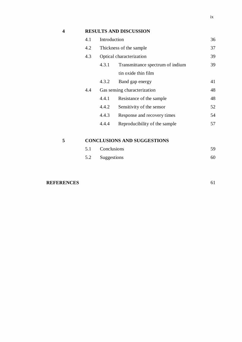
4 RESULTS AND DISCUSSION
4.1 Introduction 36
4.2 Thickness of the sample 37
4.3 Optical characterization 39
4.3.1 Transmittance spectrum of indium
tin oxide thin film
39
4.3.2 Band gap energy 41
4.4 Gas sensing characterization 48
4.4.1 Resistance of the sample 48
4.4.2 Sensitivity of the sensor 52
4.4.3 Response and recovery times 54
4.4.4 Reproducibility of the sample 57
5 CONCLUSIONS AND SUGGESTIONS
5.1 Conclusions 59
5.2 Suggestions 60
REFERENCES 61
x
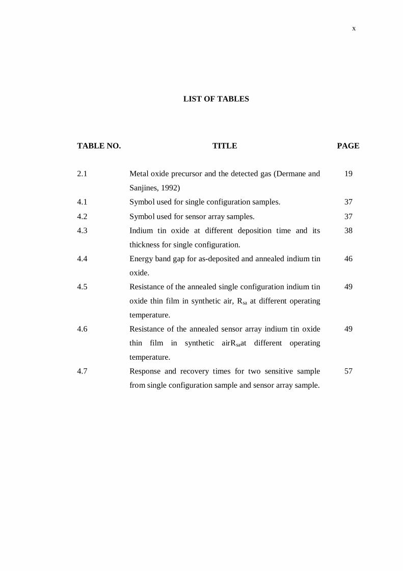
LIST OF TABLES
TABLE NO. TITLE PAGE
2.1 Metal oxide precursor and the detected gas (Dermane and
Sanjines, 1992)
19
4.1 Symbol used for single configuration samples. 37
4.2 Symbol used for sensor array samples. 37
4.3 Indium tin oxide at different deposition time and its
thickness for single configuration.
38
4.4 Energy band gap for as-deposited and annealed indium tin
oxide.
46
4.5 Resistance of the annealed single configuration indium tin
oxide thin film in synthetic air, Rsa at different operating
temperature.
49
4.6 Resistance of the annealed sensor array indium tin oxide
thin film in synthetic airRsaat different operating
temperature.
49
4.7 Response and recovery times for two sensitive sample
from single configuration sample and sensor array sample.
57
xi
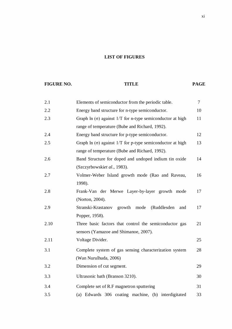
LIST OF FIGURES
FIGURE NO. TITLE PAGE
2.1 Elements of semiconductor from the periodic table. 7
2.2 Energy band structure for n-type semiconductor. 10
2.3 Graph ln (σ) against 1/T for n-type semiconductor at high
range of temperature (Bube and Richard, 1992).
11
2.4 Energy band structure for p-type semiconductor. 12
2.5 Graph ln (σ) against 1/T for p-type semiconductor at high
range of temperature (Bube and Richard, 1992).
13
2.6 Band Structure for doped and undoped indium tin oxide
(Szczyrbowskiet al., 1983).
14
2.7 Volmer-Weber Island growth mode (Rao and Raveau,
1998).
16
2.8 Frank-Van der Merwe Layer-by-layer growth mode
(Norton, 2004).
17
2.9 Stranski-Krastanov growth mode (Ruddlesden and
Popper, 1958).
17
2.10 Three basic factors that control the semiconductor gas
sensors (Yamazoe and Shimanoe, 2007).
21
2.11 Voltage Divider. 25
3.1 Complete system of gas sensing characterization system
(Wan Nurulhuda, 2006)
28
3.2 Dimension of cut segment. 29
3.3 Ultrasonic bath (Branson 3210). 30
3.4 Complete set of R.F magnetron sputtering 31
3.5 (a) Edwards 306 coating machine, (b) interdigitated 33
xii
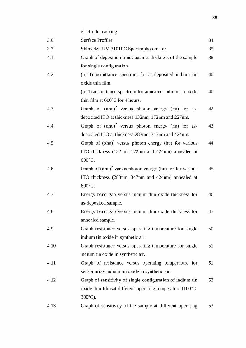
electrode masking
3.6 Surface Profiler 34
3.7 Shimadzu UV-3101PC Spectrophotometer. 35
4.1 Graph of deposition times against thickness of the sample
for single configuration.
38
4.2 (a) Transmittance spectrum for as-deposited indium tin
oxide thin film.
40
(b) Transmittance spectrum for annealed indium tin oxide
thin film at 600ºC for 4 hours.
40
4.3 Graph of (αhυ)2 versus photon energy (hυ) for as-
deposited ITO at thickness 132nm, 172nm and 227nm.
42
4.4 Graph of (αhυ)2 versus photon energy (hυ) for as-
deposited ITO at thickness 283nm, 347nm and 424nm.
43
4.5 Graph of (αhυ)2 versus photon energy (hυ) for various
ITO thickness (132nm, 172nm and 424nm) annealed at
600°C.
44
4.6 Graph of (αhυ)2 versus photon energy (hυ) for for various
ITO thickness (283nm, 347nm and 424nm) annealed at
600°C.
45
4.7 Energy band gap versus indium thin oxide thickness for
as-deposited sample.
46
4.8 Energy band gap versus indium thin oxide thickness for
annealed sample.
47
4.9 Graph resistance versus operating temperature for single
indium tin oxide in synthetic air.
50
4.10 Graph resistance versus operating temperature for single
indium tin oxide in synthetic air.
51
4.11 Graph of resistance versus operating temperature for
sensor array indium tin oxide in synthetic air.
51
4.12 Graph of sensitivity of single configuration of indium tin
oxide thin filmsat different operating temperature (100ºC-
300ºC).
52
4.13 Graph of sensitivity of the sample at different operating 53
xiii
temperature for sensor array indium tin oxide thin film.
4.14 Sample C load voltage to the function of time at 200°C
operating temperature, Vc=8V and RL=900Ω.
55
4.15 Sample H load voltage to the function of time at 250°C
operating temperature, Vc=8V and RL=900Ω.
56
4.16 Reproducibility of the sample C at 200°C operating
temperature exposed to 200ppm concentration of NO2 in 3
cycles.
57
4.17 Reproducibility of the sample H at 250°C operating
temperature exposed to 200ppm concentration of NO2 in 3
cycles.
58
xiv
LIST OF SYMBOLS
Ec - Covalent band edge
ED - Position of the donor level
EF - Fermi level position
Eg - Energy band gap
Ev - Valence band edge
R - Resistance
RL
Rsa
Rsg
-
-
-
Load resistance
Resistance of sample in synthetic air
Resistance of sample in test gas
Rs - Resistance of the sample
S - Sensitivity
T - Temperature
t - Thin film thickness
V
VC
-
-
Voltage
Supply Voltage
VL - Load Voltage
Ρ - Charge density
Φ - Work function
ᵩ (x) - Electrostatic potential
χ - Electron affinity
𝜆
ΔR
h
𝜈
𝜶
-
-
-
-
-
-
Wavelength
Resistance different
Planck's Constant
Frequency
Adsorption coefficient
CHAPTER 1
INTRODUCTION
1.1 Background of Research
Indium tin oxide, ITO or the other synonym tin-doped indium oxide is a
mixture of 90% indium oxide, In2O3 and 10% tin dioxide, SnO2 by weight
percentage. It has slightly yellow to grey colour in powder form and almost
colourless when already being deposited onto the substrate as a thin film. Nowadays,
many companies and industries used indium tin oxide in the form of thin film as a
gas sensing monitoring system in order to maintain the exposure of the toxic gasses
in the surrounding environment. Indium tin oxide has already being adapted in
almost many industries in the world because it is cost effective. Furthermore, indium
tin oxide is a very stable element and has good stability after long term usage. It also
has fast response time and very sensitive towards toxic gasses.
Indium tin oxide thin film has high optical transmittance in the visible region
that gives high conductivity. Because of the almost transparent properties of indium
tin oxide, it yield low resistivity and give good conductivity due to its addition and
increment of carrier concentration. Tin-doped indium oxide has many other
applications in industry for examples, liquid crystal display (Pankove et al., 1980),
development in television and computer screen. Besides, it also has been used in
anti-static coating, solar cell, heat mirror (Chopra et al., 1983; Hamburg et al., 1986),
light emitting diode (Kim et al., 1998), flat panel display (Lee et al., 1977) and
electroluminescent devices (Meng et al., 1987).
2
Nowadays, many techniques and methods have been used to deposit metal
oxide thin film onto the substrate such as thermal heat evaporation, pulse laser beam
exposure, chemical vapor deposition, electron beam thermal evaporation, spray
pyrolysis and radio frequency magnetron sputtering. This research work has focused
on the uses of radio frequency magnetron sputtering method to deposit indium thin
oxide, ITO thin film.
To improve the electrical properties of indium tin oxide thin film to be
functional, interdigitated aluminum electrode was deposited onto the sensing layer by
using electron beam evaporation machine. Interdigitated electrode was used in order
to enhance the sensitivity of the electrical properties and it will amplified the signal
because of the small separation between the comb-like design of a few micrometer
and less.
1.2 Statement of Problem
In the 21st century, many industries have developed rapidly, especially that
result in poor ventilation in humans such as factories that produced electronic
devices, medical devices and also universities that runned the experiments using
hazardous gases. It is very important to detect those hazardous gases precisely and
rapidly. By alerting and monitoring the presence toxic gases, it can prevent or
minimize accidents to almost 90% involving poisoning or explosions. Toxic gases,
including carbon monoxide, hydrogen sulfide, chlorine, bromine, hydrogen chloride,
hydrogen fluoride, nitric oxide, nitrogen dioxide, sulfur dioxide, ammonia, hydrogen
cyanide, phosgene, benzene, formaldehyde and methyl bromide are found in a wide
range of industries including chemical, petroleum, electronic and also coal, gas,
mines, vehicles, sewerage, waste disposal, atmosphere, houses and even battle fields.
In the past, certain color changing reagents were adopted to detect these gases by
tedious and time-consuming colorimetric or more complicated chromatographic
methods. However, in the last ten to twenty years, many techniques have progressed
3
rapidly and more sensors have been developed for the fast precise detection of
various toxic gases.
In this research, nitrogen dioxide, NO2 gas was chosen because it is one of
the most dangerous gases. Thus, to overcome this problem, indium tin oxide, ITO
thin film was fabricated to study the sensitivity of the film towards nitrogen dioxide
gas at different operating temperature in the laboratory. However, some of the
studies have high operating temperature for undoped material and also high response
times. (Steffes et al., 2000; Jaswinder Kaur et al., 2007; and Forleo et al., 2005).
1.3 Objectives of the Study
The main objective of this research is to detect the nitrogen dioxide, NO2 gas
by using indium tin oxide, ITO thin film that carried out by radio frequency
magnetron sputtering method. Therefore, the research objectives are to:
a) To deposit the indium tin oxide, ITO onto the corning glass substrate to form
thin film layer.
b) To characterize the optical properties indium tin oxide, ITO thin film.
c) To detect nitrogen dioxide, NO2 gas by using Gas Sensor Characterization
System (GSCS) for single and sensor array sample.
1.4 Significant of Research
Research towards thin film as a gas sensor will give a lot of benefits to all the
heavy industry in Malaysia especially the one that handle or contribute to producing
hazardous gasses such as nitrogen oxide, NO, carbon monoxide, CO, nitrogen
dioxide, NO2 and methane. This hazardous gas is very harmful and fatal to human
being and will caused chronic diseases such as asthma, brain cancer, chemical
4
poisoning and genetic damage. Thus, this research is to prevent these accidents from
occuring.
1.5 Scope of the Study
The scope of this research can be divided into five major aspects. The first
aspect was to prepare the indium tin oxide thin film by using radio frequency
magnetron sputtering at different thickness that was varied by the deposition times
which were 15, 30, 45, 60, 75 and 90 minutes.
The second aspect was to apply the heat treatment to indium tin oxide thin
film by setting the temperature to 600°C for 4 hours. The purpose of the heat
treatment was to produce the fine thin film structure to enhance the electrical
properties due to its decrements in resistivity and increase the conductivity by
increasing of carrier concentration. This is because the thin film structure already
transform from amorphous to crystal (Bhatti et.al., 2002).
The third aspect was to deposit the pair of aluminium interdigitated comb-like
electrodes onto the thin film in order to amplify the electrical signal to be detected.
The fourth aspect was to characterize the prepared thin film by using UV-Vis
spectroscopy and surface profiler to determine the exact thickness. The last aspect
was to detect nitrogen dioxide, NO2 gas by using indium thin oxide, ITO thin film
using the Gas Sensor Characterization System (GSCS). The samples were divided
into two categories, single configuration samples and sensor array combination.
61
REFERENCES
Balasubramanium, N. and Subramanyam, A. (1988). Effect of Substrate Temperature
on the Electrical and Optical Properties of Reactively Evaporated Indium Tin
Oxide Films. Material Science and Engineering. B1., pp. 279-281
Bube and Richard, H., (1992). Electrons in Solids:An Introduction Survey. 3rd
Edition, California:Academic Press Inc.
Chopra, K.L., Major, S. and Panday, D.K. (1983). Thin Solid Films. 102.
Chopra, K.L., Major, S. and Pandya, D.K. (1983). Transparent Conductor - A status
Review. Thin Solid Films. 102., pp. 1-46
Demarne, V. and Sanjines, R. (1992). Thin Film Semiconducting Metal Oxide Gas
Sensor. Gas Sensor-Principles, Operation And Developments,
London:Kluwer Academic. pp. 89-116
Dunlap, W.C. (1957). An Introduction to Semiconductor. Wiley, New York. pp 96
Fan, J.C.C. and Goodenough. (1977). X-Ray Photoemission Spectroscopy Studies of
Sndoped Indium Oxide Films. Journal of Applied Physics. pp. 3524-3531
Forleo. A, Francioso. L, Epifani. M,Copone. S, Taurino. A. M, and Siciliano. P.
(2005). NO2-gas sensing properties of mixed In2O3-SnO2 thin films. Thin
Solid Films.
Gospel, W. and Scierbaum, K.D. (1995). SnO2 sensors:current status and future
prospects. sensors and actuators. B 26-27., pp. 1-12
62
Gupta, L., Mansingh, A. and Srivastava, P.K. (1989). Narrowing and the Band
Structure of Tin Doped Indium Oxide Films. Thin Solid Films. 176., pp. 33-
44
Hamburg, C.G. and Granquist. (1986). J. Applied Physics. R123.60
Henish, H.K. (1957). Rectifying Semiconductor Contacts. Oxford Univ. Press
London and New York. pp 251
Jaswinder Kaur, Somnath Roy. C, and Bhatnagar. M. C. (2007). Highly sensitive
SnO2 thin film NO2 gas sensor operating at low temperature. Sensors and
Actuators B.
Kim, J.S., Granstorm, M., Friend, R.H., Johansson, N., Salaneck, W.R., Daik, R.,
Feast, W.J. and Cacialli, F. (1998). J. Applied Physics. 84.6859
Lee, B.H., Kim, I.G., Cho, S.W. and Lee, S.H. (1977). Thin Solid Films. 25.302
Meng, L.J., Li, C.H., Zhong, G.Z. and Lumin. J. (1987). 11
Muhammad Yahaya. (1997). Teknologi Filem Nipis. Cetakan Pertama,
Selangor:Universiti Kebangsaan Malaysia.pp 30
Norton, D. (2004). Mater. Sci. Eng. R 43-139
Pankove, J.I., (1980). Topic in Applied Physics, Springer, Berlin. vol. 40
Patel, N.G., Panchal, C.J., and Makhija, K.K. (1994). Use of Cadmium Selenide Thin
Film as a Carbon Dioxide Gas Sensor. Cryst. Res. Technol. 29., pp. 1013-
1020
Rao, C.N.R., Raveau, B. (1998). Transition Metal Oxide, 2nd edn. Wiley-VCH, New
York. pp220
63
Ruddlesden, S.N. and Popper, P. (1958). Acta. Crystallogr. 11-54
Shamsuri, W.N.W. (2006). Development of Carbon Monoxide Gas Sensing System
Using Tin Oxide Thin Films As a sensor. Universiti Teknologi Malaysia,
Skudai, PhD Thesis.
Steffes. H, Imawan. C, Solzbacher. F and Obermeier. E. (2000). Fabrication
parameters and NO2 sensitivity of reactively RF-sputtered In2O3 thin films.
Sensors and Actuators B.
Szczyrbowski, J., Dietrich, A. and Hoffman, H. (1983). Optical and Electrical
Properties of R.F. Sputtered Indium-Tin Oxide Films. Phys Stat Sol (a). 78.,
pp. 243-252
Tariq Bhatti, M., Anwar Manzoor Rana., Abdul Faheem Khan and Iqbal Ansari, M.,
(2002). Effect of Annealing on Electrical Properties of Indium Tin Oxide
(ITO) Thin Film. Pakistan Journal of Applied Sciences. 2(5):570-573.
Theodor, D. (2003). Semiconducting Oxides as Gas Sensitive Resistors. sensor and
actuator. B 57., pp. 1-16
Turnbull, W.R. (1968). Semiconducting Thin Films. an annotated bibliography,
NOLC Rept. 712-745
Yacobi, B.G. (2003). An Introduction to Basic Principles. Semiconductor Materials.
ISBN 0306473615., pp. 1-3
Yamazoe, N. and Shimanoe, K. (2007). Overview of gas sensor technology. Science
and Technology of Chemiresistor Gas Sensor, Nova Publisher Inc.
Zhang Xin, Song Xia Hui, Zhang Dian-Lin. (2010). Thickness Dependance of Grain
size and Surface Roughness for dc magnetron sputtered Au films. Chin. Phys.
B.